SLVUBD4B January 2018 – October 2020 TPS27SA08
4 HSS-MOTHERBOARDEVM EVM Assembly Drawings and Layout
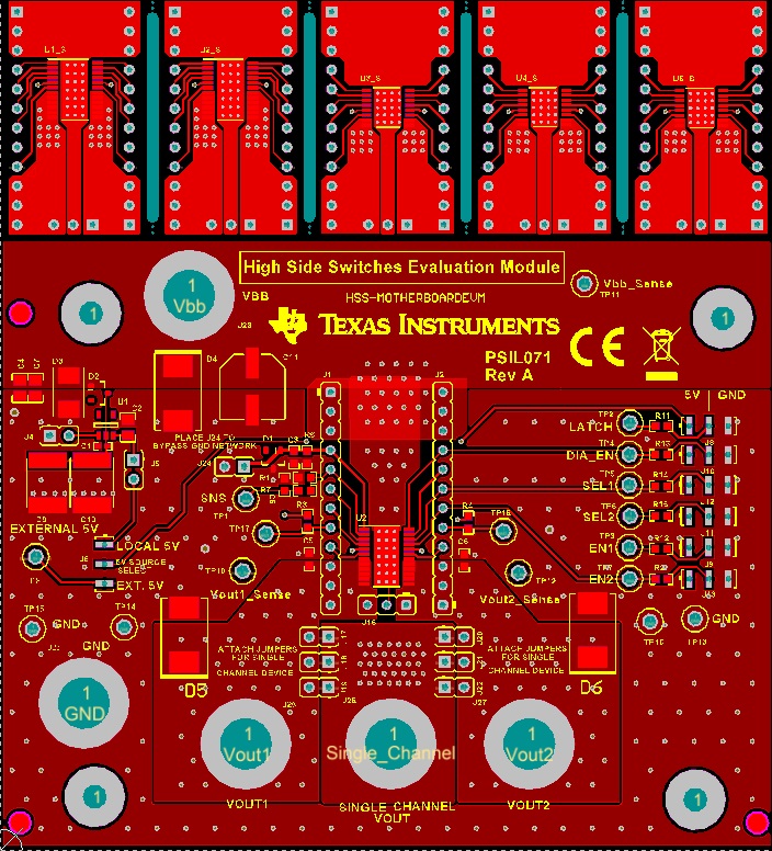
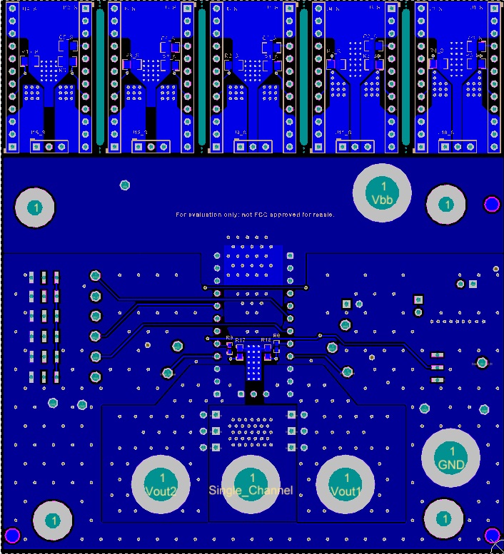
Figure 4-1 show the design of the HSS-MOTHERBOARDEVM and daughterboard PCB. The EVM was designed using FR4 material on a two-layer board. All components are located in an active area on the top side and active traces are provided in the top and bottom layers to allow the user to easily view, probe, and evaluate. Moving components to both sides of the PCB can offer additional size reduction for space-constrained systems.
 Figure 4-1 HSS-MOTHERBOARDEVM Layout and Routing (Top View)
 Figure 4-2 HSS-MOTHERBOARDEVM Layout and Routing (Bottom View)