SLVAEX3 October   2020 TPS8802 , TPS8804


  1.   Trademarks
  2. 1Introduction
  3. 2SNR Optimization
    1. 2.1 SNR Overview
    2. 2.2 Smoke Concentration Measurement
    3. 2.3 Amplifier and LED Settings
      1. 2.3.1 Photo Amplifier Gain
      2. 2.3.2 Photo Amplifier and AMUX Speed
      3. 2.3.3 LED Current and Pulse Width
    4. 2.4 ADC Sampling and Digital Filtering
      1. 2.4.1 ADC Sampling
      2. 2.4.2 Digital Filtering
  4. 3System Modeling
    1. 3.1 Impulse Response
      1. 3.1.1 Photodiode Input Amplifier Model
      2. 3.1.2 Photodiode Gain Amplifier and AMUX Buffer Model
      3. 3.1.3 Combined Signal Chain
    2. 3.2 Noise Modeling
      1. 3.2.1 Noise Sources
      2. 3.2.2 Output Voltage Noise Model
      3. 3.2.3 ADC Quantization Noise
    3. 3.3 SNR Calculation
      1. 3.3.1 Single ADC Sample
      2. 3.3.2 Two ADC Samples
      3. 3.3.3 Multiple Base ADC Samples
      4. 3.3.4 Multiple Top ADC Samples
      5. 3.3.5 Multiple ADC Sample Simulation
  5. 4SNR Measurements
    1. 4.1 Measurement Procedure
    2. 4.2 Measurement Processing
    3. 4.3 Measurement Results
      1. 4.3.1 Varying Amplifier Speeds
      2. 4.3.2 Varying Digital Filter and ADC Timing
      3. 4.3.3 Varying LED Pulse Length
      4. 4.3.4 Varying ADC Sample Rate
      5. 4.3.5 Real and Ideal System Conditions
      6. 4.3.6 Number of Base Samples
      7. 4.3.7 ADC Resolution
  6. 5Summary
  7. 6References

ADC Quantization Noise

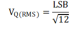
ADC quantization noise is a noise source caused by rounding the photo signal to the nearest least significant bit (LSB) when digitizing the signal. Ensure the quantization noise level is less than the photo noise level to maximize SNR. This can be done by increasing the gain in the photo input amplifier or photo gain stage. ADC quantization noise is calculated in Equation 16.

Equation 16. GUID-20200930-CA0I-PQFM-BTRH-3J74GJK33H2D-low.gif