SLVAEX3 October   2020 TPS8802 , TPS8804


  1.   Trademarks
  2. 1Introduction
  3. 2SNR Optimization
    1. 2.1 SNR Overview
    2. 2.2 Smoke Concentration Measurement
    3. 2.3 Amplifier and LED Settings
      1. 2.3.1 Photo Amplifier Gain
      2. 2.3.2 Photo Amplifier and AMUX Speed
      3. 2.3.3 LED Current and Pulse Width
    4. 2.4 ADC Sampling and Digital Filtering
      1. 2.4.1 ADC Sampling
      2. 2.4.2 Digital Filtering
  4. 3System Modeling
    1. 3.1 Impulse Response
      1. 3.1.1 Photodiode Input Amplifier Model
      2. 3.1.2 Photodiode Gain Amplifier and AMUX Buffer Model
      3. 3.1.3 Combined Signal Chain
    2. 3.2 Noise Modeling
      1. 3.2.1 Noise Sources
      2. 3.2.2 Output Voltage Noise Model
      3. 3.2.3 ADC Quantization Noise
    3. 3.3 SNR Calculation
      1. 3.3.1 Single ADC Sample
      2. 3.3.2 Two ADC Samples
      3. 3.3.3 Multiple Base ADC Samples
      4. 3.3.4 Multiple Top ADC Samples
      5. 3.3.5 Multiple ADC Sample Simulation
  5. 4SNR Measurements
    1. 4.1 Measurement Procedure
    2. 4.2 Measurement Processing
    3. 4.3 Measurement Results
      1. 4.3.1 Varying Amplifier Speeds
      2. 4.3.2 Varying Digital Filter and ADC Timing
      3. 4.3.3 Varying LED Pulse Length
      4. 4.3.4 Varying ADC Sample Rate
      5. 4.3.5 Real and Ideal System Conditions
      6. 4.3.6 Number of Base Samples
      7. 4.3.7 ADC Resolution
  6. 5Summary
  7. 6References

Varying ADC Sample Rate

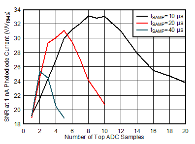
The ADC sample rate is determined by the microcontroller, clock speeds, and sample and hold times. While there may not be much adjustability of the ADC sample rate in a system, it is important to consider the effects of sample rate on the SNR. Three ADC sample rates are used to calculate the SNR, shown in Figure 4-17. Decreasing the ADC sampling interval from 40 μs to 20 μs to 10 μs increases the maximum attainable SNR from 25.4 to 31.1 to 33.1. The benefit of taking multiple top ADC samples decreases as the ADC sampling interval increases. As the ADC sampling interval approaches the LED pulse width, reduce the number of top ADC samples and increase τ1 and τ2.
GUID-20200930-CA0I-VDHL-XCVD-D4PMCV23VR5P-low.gif

tLED=100 µs τ1=15 µs τ2=15 µs

Figure 4-17 SNR at 1 nA with Optimal Averaging Filter Varying ADC Sample Interval