SLVAEX3 October   2020 TPS8802 , TPS8804


  1.   Trademarks
  2. 1Introduction
  3. 2SNR Optimization
    1. 2.1 SNR Overview
    2. 2.2 Smoke Concentration Measurement
    3. 2.3 Amplifier and LED Settings
      1. 2.3.1 Photo Amplifier Gain
      2. 2.3.2 Photo Amplifier and AMUX Speed
      3. 2.3.3 LED Current and Pulse Width
    4. 2.4 ADC Sampling and Digital Filtering
      1. 2.4.1 ADC Sampling
      2. 2.4.2 Digital Filtering
  4. 3System Modeling
    1. 3.1 Impulse Response
      1. 3.1.1 Photodiode Input Amplifier Model
      2. 3.1.2 Photodiode Gain Amplifier and AMUX Buffer Model
      3. 3.1.3 Combined Signal Chain
    2. 3.2 Noise Modeling
      1. 3.2.1 Noise Sources
      2. 3.2.2 Output Voltage Noise Model
      3. 3.2.3 ADC Quantization Noise
    3. 3.3 SNR Calculation
      1. 3.3.1 Single ADC Sample
      2. 3.3.2 Two ADC Samples
      3. 3.3.3 Multiple Base ADC Samples
      4. 3.3.4 Multiple Top ADC Samples
      5. 3.3.5 Multiple ADC Sample Simulation
  5. 4SNR Measurements
    1. 4.1 Measurement Procedure
    2. 4.2 Measurement Processing
    3. 4.3 Measurement Results
      1. 4.3.1 Varying Amplifier Speeds
      2. 4.3.2 Varying Digital Filter and ADC Timing
      3. 4.3.3 Varying LED Pulse Length
      4. 4.3.4 Varying ADC Sample Rate
      5. 4.3.5 Real and Ideal System Conditions
      6. 4.3.6 Number of Base Samples
      7. 4.3.7 ADC Resolution
  6. 5Summary
  7. 6References

Combined Signal Chain

The signal at the buffered AMUX output can be calculated using the models for each stage, as shown in Equation 7. τ1 and τ2 represent the photo input amplifier and AMUX filter time constants, respectively. Taking an integral and inverse Laplace transform of Equation 7 results in the time-dependent step response in Equation 8. Here, H(t) is the Heaviside step function, taking the value 0 for negative inputs and 1 for non-negative inputs. The step response assumes that the photocurrent is stepped from 0 to IPD when t is equal to 0. The step response calculation in Equation 8 is undefined when τ1 and τ2 are equal. In this case, the limit can be taken to solve for the step response.

Equation 7. V B U F = V P D O × G P G A I N 1 + s × R A M U X × C A M U X = I P D × 2 × R P H × G P G A I N 1 + s × τ 1 × ( 1 + s × τ 2 )
Equation 8. V B U F S T E P t = I P D × 2 × R P H × G P G A I N × 1 + τ 1 τ 2 - τ 1 × e - t τ 1 + τ 2 τ 1 - τ 2 × e - t τ 2 × H t + V D C

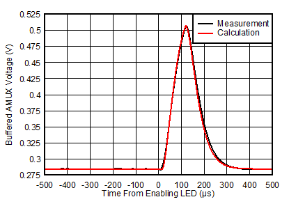
With the step response calculated, the response to a rectangular pulse input is calculated in Equation 9, where tLED is the LED pulse width. Equation 10 and Equation 11 calculate the baseline DC voltage of the buffered photo signal with and without a 470 kΩ resistor installed on PREF. VPDO(OFS) is the DC offset caused by the photo input amplifier and VPGAIN(OFS) is the DC offset caused by the photo gain amplifier. Because there is a propagation delay on the TPS880x LED driver, the output may be shifted from when the LED is enabled.
Equation 9. V B U F P U L S E ( t ) = V B U F S T E P t - V B U F S T E P t - t L E D + V D C
Equation 10. V D C = 50   m V + 5   m V + V P D O O F S + V P G A I N O F S × G P G A I N
Equation 11. V D C ( 470 k Ω ) = 70   m V + 7   m V + V P D O O F S + V P G A I N O F S × G P G A I N
GUID-20200929-CA0I-QNM6-JR3C-3W1C9MF2WXKW-low.gif

τ1=33 µs τ2=30 µs

Figure 3-3 Measurement and Amplitude-Adjusted Calculation of a 100 µs LED Photo Pulse