SLUUC85B June   2020  – September 2020 TPS62860 , TPS62861


  1.   Trademarks
  2. 1Introduction
    1. 1.1 Background
    2. 1.2 Performance Specification
    3. 1.3 Modifications
      1. 1.3.1 IC U1 Operation
  3. 2Setup
    1. 2.1 Input and Output Connector Description
      1. 2.1.1 J1, Pin 1 and 2 – VIN
      2. 2.1.2 J1, Pin 3 and 4 – S+/S-
      3. 2.1.3 J1, Pin 5 and 6 – GND
      4. 2.1.4 J2, Pin 1 and 2 – VOUT
      5. 2.1.5 J2, Pin 3 and 4 – S+/S-
      6. 2.1.6 J2, Pin 5 and 6 – GND
      7. 2.1.7 J3 – I2C
      8. 2.1.8 JP1 – EN
      9. 2.1.9 JP2 – VSEL
    2. 2.2 Setup
  4. 3Board Layout
    1. 3.1 Layout
  5. 4Schematic and Bill of Materials
    1. 4.1 Schematic
    2. 4.2 Bill of Materials
  6. 5Software User Interface
    1. 5.1 Software Setup
    2. 5.2 Interface Hardware Setup
    3. 5.3 User Interface Operation
      1. 5.3.1 Home Screen
      2. 5.3.2 Settings Screen
      3. 5.3.3 Register Map Screen
  7.   Revision History

Register Map Screen

The Register Map screen shows bit values of all parameters. In this section, single registers can be read or written to the device (if applicable). Refer to the register map in the TPS62860, TPS62861 1.8-V to 5.5-V Input, 1-A Synchronous Step-Down Converter Data Sheet for a detailed description of the TPS6286x0 registers.
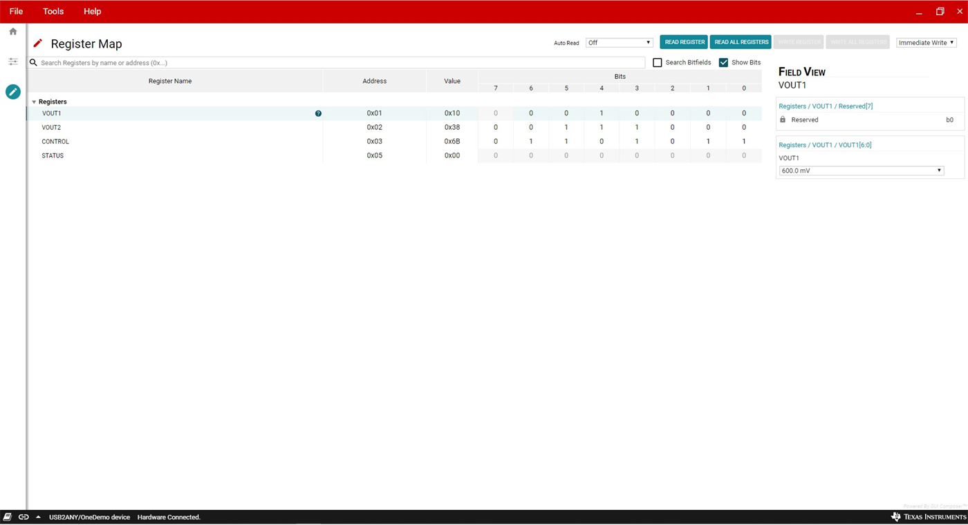
GUID-76EAA5DB-A739-438D-A926-F3271DAB1A49-low.png Figure 5-4 GUI Register Map Screen