SLUUC85B June   2020  – September 2020 TPS62860 , TPS62861


  1.   Trademarks
  2. 1Introduction
    1. 1.1 Background
    2. 1.2 Performance Specification
    3. 1.3 Modifications
      1. 1.3.1 IC U1 Operation
  3. 2Setup
    1. 2.1 Input and Output Connector Description
      1. 2.1.1 J1, Pin 1 and 2 – VIN
      2. 2.1.2 J1, Pin 3 and 4 – S+/S-
      3. 2.1.3 J1, Pin 5 and 6 – GND
      4. 2.1.4 J2, Pin 1 and 2 – VOUT
      5. 2.1.5 J2, Pin 3 and 4 – S+/S-
      6. 2.1.6 J2, Pin 5 and 6 – GND
      7. 2.1.7 J3 – I2C
      8. 2.1.8 JP1 – EN
      9. 2.1.9 JP2 – VSEL
    2. 2.2 Setup
  4. 3Board Layout
    1. 3.1 Layout
  5. 4Schematic and Bill of Materials
    1. 4.1 Schematic
    2. 4.2 Bill of Materials
  6. 5Software User Interface
    1. 5.1 Software Setup
    2. 5.2 Interface Hardware Setup
    3. 5.3 User Interface Operation
      1. 5.3.1 Home Screen
      2. 5.3.2 Settings Screen
      3. 5.3.3 Register Map Screen
  7.   Revision History

Home Screen

The Home screen provides a short overview of the TPS6286x0 devices. To start evaluating the device, click the Start button. Click the I2C Slave Address button to change the address, and the default I2C address is 0x40. All the links related to the device are all indicated on the bottom portion of the window.
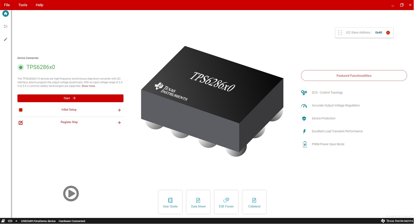
GUID-5B88BBEB-8CC4-4CA2-A536-EFCB1FB62E60-low.png Figure 5-2 GUI Home Screen