SLAA996A June 2021 – June 2021 TPA6304-Q1
- Trademarks
- 1Introduction
- 2Understanding the Thermal Flow
- 3Understanding the Test and System Conditions
- 4Calculating Dynamic Thermal Dissipation
- 5Designing a Realistic Thermal Test
- 6Thermal Tests
- 7Overall Summary
- 8References
- 9Revision History
2 Understanding the Thermal Flow
The equation used for calculating the thermal dissipation of a system is shown in Equation 1:
Where:
- θJA = thermal resistance
- TJ = junction temperature
- TA = ambient temperature
- PD = power dissipation
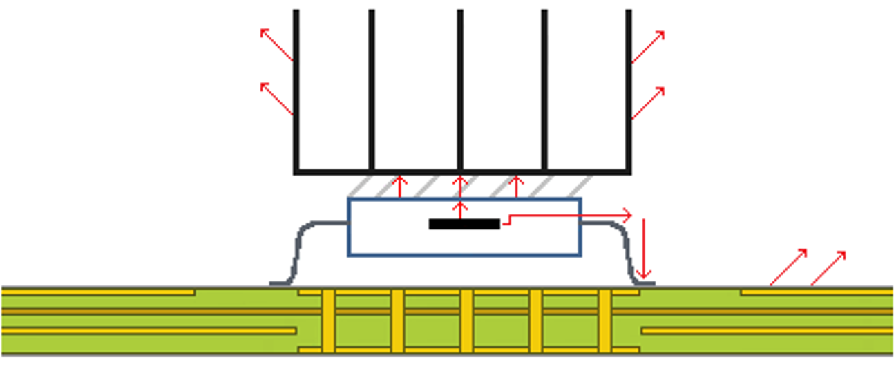
θJA represents the thermal resistance path(s) where the heat will flow out of the amplifier to relatively cooler surroundings. There are two paths where the heat generated from the device can go. As seen in Figure 2-1, for top-mounted heatsinks, heat can escape from the junction to the thermal pad (case), then to the thermal interface material. From the thermal interface material the heat goes to the heatsink, then through the heatsink to the surrounding air. The second path is from the junction to the board, then from the board to surrounding air.
 Figure 2-1 Thermal Model
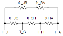
Using thermal dissipation equations, the thermal model seen in Figure 2-1 can be represented as shown in Figure 2-2 where:
- θJC = thermal resistance of the device from the junction to the case
- θCH = thermal resistance of the interface compound
- θHA = thermal resistance of the heatsink
- θJB = thermal resistance of the device from the junction to the board
- θBA = thermal resistance of the board
 Figure 2-2 Thermal Resistance
Model
Figure 2-2 Thermal Resistance
ModelThis can be simplified as the majority of the heat from the device will be going through the case into the heatsink rather than from the package to the board as θJC, θCH, and θHA have a much lower combined thermal resistance to that of θJB and θBA. The simplified thermal resistance model is shown in Figure 2-3.
 Figure 2-3 Simplified Thermal Resistance
Model
Figure 2-3 Simplified Thermal Resistance
ModelWith the simplified thermal resistance model, the thermal dissipation equation can be written as:
Since θJC represents the intrinsic thermal properties between the junction and case of the device, it cannot be changed. θCH and θHA will vary greatly from system to system depending on the materials chosen for the heatsink, weight and shape of the heatsink, thickness of the thermal gap filler, and the thermal resistance of the thermal gap filler.