SLAA517F May 2012 – August 2021 MSP430F6720A , MSP430F6720A , MSP430F6721A , MSP430F6721A , MSP430F6723A , MSP430F6723A , MSP430F6724A , MSP430F6724A , MSP430F6725A , MSP430F6725A , MSP430F6726A , MSP430F6726A , MSP430F6730A , MSP430F6730A , MSP430F6731A , MSP430F6731A , MSP430F6733A , MSP430F6733A , MSP430F6734A , MSP430F6734A , MSP430F6735A , MSP430F6735A , MSP430F6736 , MSP430F6736 , MSP430F6736A , MSP430F6736A
3.2.2 Current Inputs
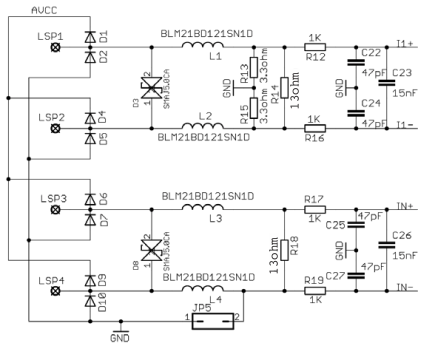
The analog front-end for current inputs is a little different from the analog front end for the voltage inputs. Figure 3-3 shows the analog front end used for the current channels I1 and I2.
 Figure 3-3 Analog Front End for Current Inputs
Resistors R14 and R18 are the burden resistors that would be selected based on the current range used and the turns-ratio specification of the CT (not required for shunt). The value of the burden resistor for this design is around 13 Ω. The anti-aliasing circuitry consisting of R and C follows the burden resistor. The input signal to the converter is a fully differential input with a voltage swing of ±920 mV maximum with gain of the converter set to 1. Similar to the voltage channels, the common mode voltage is selectable to either analog ground (GND) or internal reference on channels connected to LSP3 and LSP4.