SFFS422 May 2022
- Trademarks
- 2
- 1Scope
- 2Related Documents
- 3Related Standards and Acronyms
-
4Concept Overview
- 4.1 System Block Diagram
- 4.2 System Specifications
- 4.3 Conditions of use: Assumptions
- 4.4 Safe Torque Off Implementation
- 4.5 Safe State
- 5Concept FMEA
- 6References
4.4.7.2 Load Switch: TPS22919
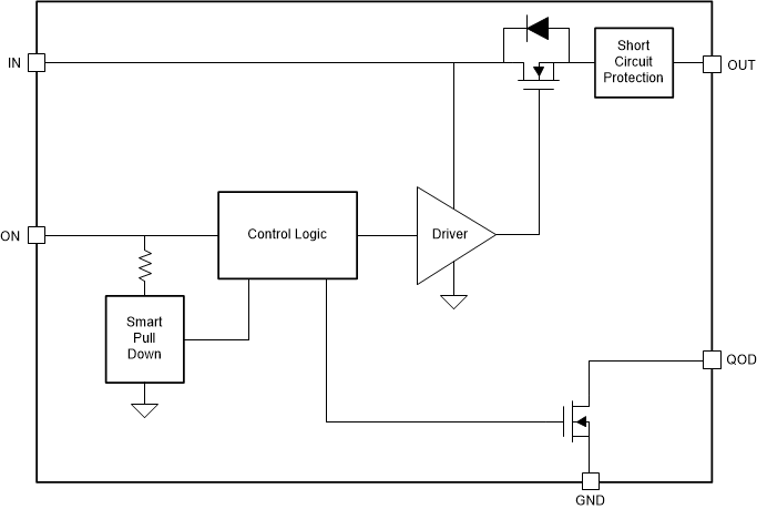
 Figure 4-9 TPS22919 Block Diagram
Table 4-5 describes the connection of the VOUT pin depending on the state of the ON pin as well as the various QOD pin configurations.
Table 4-5 TPS22919 Functional Modes vs
QOD
| On | QOD Configuration | TPS22919 VOUT |
|---|---|---|
| L | QOD pin connected to VOUT with RQOD | GND (RPD, QOD + RQOD) |
| L | QOD pin tied to VOUT directly | GND (RPD, QOD) |
| L | QOD pin left open | Floating |
| H | N/A | VIN |