SFFS422 May 2022
- Trademarks
- 2
- 1Scope
- 2Related Documents
- 3Related Standards and Acronyms
-
4Concept Overview
- 4.1 System Block Diagram
- 4.2 System Specifications
- 4.3 Conditions of use: Assumptions
- 4.4 Safe Torque Off Implementation
- 4.5 Safe State
- 5Concept FMEA
- 6References
4.4.7.4 Isolated Gate Driver: ISO5852S (ISO5452)
 Block
Diagram") Figure 4-11 ISO5852S (ISO5452) Block
Diagram
Figure 4-11 ISO5852S (ISO5452) Block
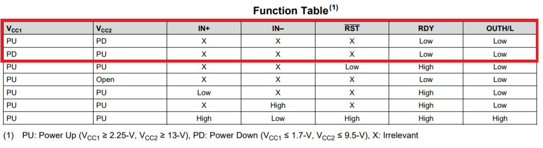
DiagramTable 4-6 shows the ISO5852S (ISO5452) isolated gate driver output voltage depending on the logic supply voltage VCC1 and the isolated supply voltage VCC2. If any of these supply voltages is off (see threshold values under footnote 1), the output OUTH/L of the gate driver is low. Table 4-6 is copied from the ISO5852S (ISO5452) data sheet, reference number SLLSEQ0 and SLLSEQ4.
Table 4-6 ISO5852S (ISO5452) Functional Table VCC1 and VCC2/VEE2 vs Output Voltage
 |