SBOU274 December 2021 OPT3004
5.2.1 Schematic
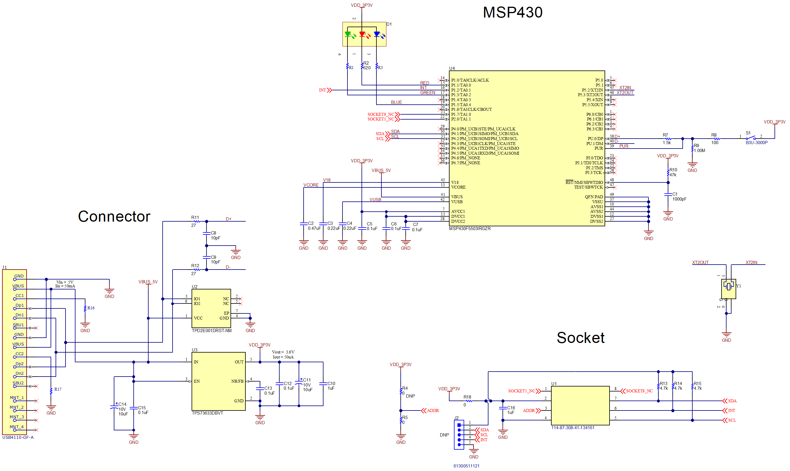
Figure 5-1 shows the complete schematic of the OPTMBEVM motherboard. The schematic is split into three sections: connector, MSP430, and socket. A USB type C connector is used to interface with the PC. The MSP430 microcontroller allows the PC to interface with the OPT3004DTS through I2C. The coupon board containing the OPT3004DTS plugs into the motherboard through the socket. The OPTMBEVM board provides easy access to the I2C, INT, VDD, and GND lines. The header J2 is depopulated on the EVM by default and its labeled through hole pads can be used to access the lines. Alternatively, a header can be populated at J2 for easier access.
 Figure 5-6 OPTMBEVM Schematic