SBOU274 December 2021 OPT3004
5.2.2 PCB Layout
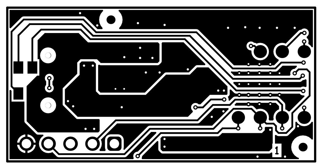
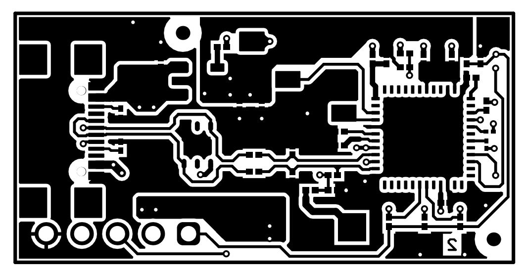
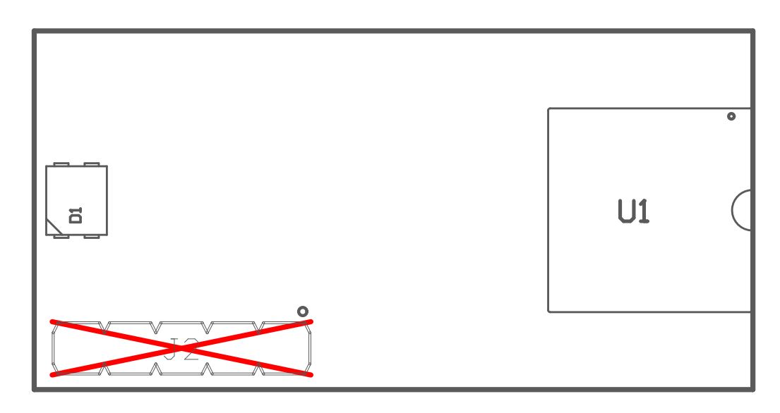
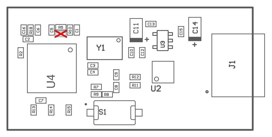
Figure 5-2 and Figure 5-3 show the top and bottom PCB layers, respectively, of the test board. Figure 5-4 and Figure 5-5 show the assembly drawings of the top and bottom PCB layers, respectively.
 Figure 5-7 PCB Top
Layer
 Figure 5-8 PCB
Bottom Layer
 Figure 5-9 PCB Top-Layer Assembly
Drawing
 Figure 5-10 PCB Bottom-Layer Assembly
Drawing