SBOU192 July 2017
-
DIYAMP-SC70-EVM
- Trademarks
- 1 Introduction
- 2 Hardware Setup
- 3
Schematic and PCB Layout
- 3.1 Schematic PCB Drawing
- 3.2 Single-Supply, Multiple Feedback Filter
- 3.3 Single-Supply, Sallen-Key Filter
- 3.4 Single-Supply, Non-Inverting Amplifier
- 3.5 Single-Supply, Inverting Amplifier
- 3.6 Difference Amplifier
- 3.7 Dual-Supply, Multiple Feedback Filter
- 3.8 Dual-Supply, Sallen-Key Filter
- 3.9 Inverting Comparator
- 3.10 Non-Inverting Comparator
- 3.11 Riso With Dual Feedback
- 3.12 Dual-Supply, Non-Inverting Amplifier
- 3.13 Dual-Supply, Inverting Amplifier
- 4 Connections
- 5 Bill of Materials and Reference
3.11 Riso With Dual Feedback
Figure 36 shows the schematic for the Riso with dual-feedback circuit configuration.
 Figure 36. Riso with Dual-Feedback Schematic
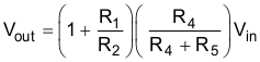
 The dc gain of the Riso with dual-feedback circuit configuration can be calculated using Equation 24.
In situations where stability is affected by capacitive loads, the Riso dual-feedback configuration has the ability to stabilize the circuit by compensating the contribution of the capacitive load to circuit instability. This capacitive load compensation technique uses an isolation resistor that compensates the circuit by adding a zero to cancel the pole from the output impedance and capacitive load. Refer to the TI Precision Labs - Op Amps: Stability 5 video for detailed information on this technique.
The design steps for the Riso method follow:
- Use TINA-TI™ to find the zero frequency, fZERO, where AOL_Loaded = 20 dB (example shown in Figure 37).
- Calculate Riso to set the zero at fZERO – this will yield between 60° and 90° of phase margin
- Riso = R3
- CLoad = C4
 Figure 37. Example of fZERO, Where AOL_Loaded = 20 dB
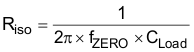
where
While the Riso circuit is both simple to implement and design, it has a big disadvantage in precision circuits. The voltage drop from Riso is dependent on the output current or output load, and may be significant compared to the desired signal.
The second capacitive load compensation technique uses the Riso with dual-feedback stability compensation method. The Riso dual-feedback circuit solves the voltage drop disadvantage of the previously stated Riso. Refer to the TI Precision Labs - Op Amps: Stability 6 video for detailed information on this technique.
Design steps for the Riso method follow:
- Riso using Method 1: Riso techniques
- Set R1: R1 ≥ (Riso × 100)
- Set C1:
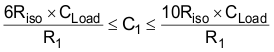
Using this range ensures that the two feedback paths, R2 and C3, will never create a resonance that would cause instability. Smaller values of C3 will result in faster settling time at the expense of overshoot for certain load ranges. While the Riso dual-feedback circuit solves the dc accuracy issue with the Riso circuit, it has some disadvantages as well. The disadvantage of this method is that the circuit is not as tolerant to changes in the output capacitance and can quickly become unstable. Therefore, the Riso dual-feedback circuit is best for situations where the output capacitance is known and will not vary significantly. This method generally results in a slower settling time than the Riso circuit as well.
The PCB layout of the top layer of the Riso dual-feedback amplifier circuit configuration is displayed in Figure 38
 Figure 38. Riso Dual-Feedback Top Layer
 The PCB layout of the bottom layer of the Riso dual-feedback amplifier circuit configuration is displayed in Figure 39.
 Figure 39. Riso Dual-Feedback Bottom Layer