SBOU192 July 2017
-
DIYAMP-SC70-EVM
- Trademarks
- 1 Introduction
- 2 Hardware Setup
- 3
Schematic and PCB Layout
- 3.1 Schematic PCB Drawing
- 3.2 Single-Supply, Multiple Feedback Filter
- 3.3 Single-Supply, Sallen-Key Filter
- 3.4 Single-Supply, Non-Inverting Amplifier
- 3.5 Single-Supply, Inverting Amplifier
- 3.6 Difference Amplifier
- 3.7 Dual-Supply, Multiple Feedback Filter
- 3.8 Dual-Supply, Sallen-Key Filter
- 3.9 Inverting Comparator
- 3.10 Non-Inverting Comparator
- 3.11 Riso With Dual Feedback
- 3.12 Dual-Supply, Non-Inverting Amplifier
- 3.13 Dual-Supply, Inverting Amplifier
- 4 Connections
- 5 Bill of Materials and Reference
3.13 Dual-Supply, Inverting Amplifier
Figure 43 shows the schematic for the dual-supply, inverting amplifier circuit configuration.
 Figure 43. Dual-Supply, Inverting Amplifier Schematic
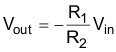
 The inverting op-amp configuration takes an input signal that is applied directly to the inverting input terminal and outputs a signal that is the opposite polarity as the input signal. The benefit of this topology is that it avoids common mode limitations. The load resistance for this topology is equal to R2. The values of the resistors in the feedback network will determine the amount of gain to amplify the input signal.
Equation 28 displays the transfer function for the dual-supply, inverting amplifier circuit configuration shown in Figure 43.
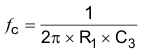
Capacitor C3 provides the option to filter the output. The cutoff frequency of the filter can be calculated using Equation 29.
The PCB layout of the top layer of the dual-supply, inverting amplifier circuit configuration is displayed in Figure 44.
 Figure 44. Dual-Supply, Inverting Amplifier Top Layer
 The PCB layout of the bottom layer of the dual-supply, inverting amplifier circuit configuration is displayed in Figure 45.
 Figure 45. Dual-Supply, Inverting Amplifier Bottom Layer