SBOU192 July 2017
-
DIYAMP-SC70-EVM
- Trademarks
- 1 Introduction
- 2 Hardware Setup
- 3
Schematic and PCB Layout
- 3.1 Schematic PCB Drawing
- 3.2 Single-Supply, Multiple Feedback Filter
- 3.3 Single-Supply, Sallen-Key Filter
- 3.4 Single-Supply, Non-Inverting Amplifier
- 3.5 Single-Supply, Inverting Amplifier
- 3.6 Difference Amplifier
- 3.7 Dual-Supply, Multiple Feedback Filter
- 3.8 Dual-Supply, Sallen-Key Filter
- 3.9 Inverting Comparator
- 3.10 Non-Inverting Comparator
- 3.11 Riso With Dual Feedback
- 3.12 Dual-Supply, Non-Inverting Amplifier
- 3.13 Dual-Supply, Inverting Amplifier
- 4 Connections
- 5 Bill of Materials and Reference
3.7 Dual-Supply, Multiple Feedback Filter
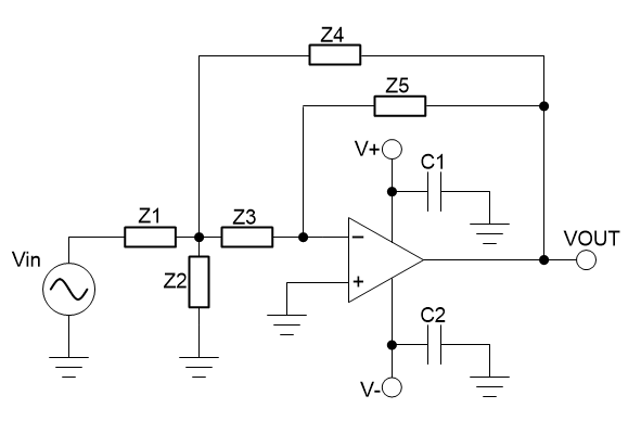
Figure 24 shows the schematic for the dual-supply, multiple feedback filter circuit configuration.
 Figure 24. Dual-Supply, Multiple Feedback Filter Schematic
 The MFB topology (sometimes called infinite gain or Rauch) is often preferred due to low sensitivity to component variations. The MFB topology creates an inverting second-order stage. This inversion may, or may not, be a concern in the filter application.
The dual-supply, MFB filter circuit can be configured as a low-pass filter, high-pass filter, or band-pass filter based on the component selection of Z1 through Z5. Table 5 displays the type of passive component that should be chosen for Z1 through Z5 for each filter configuration.
Table 5. MFB Filter Type Component Selection
| Pass-Band
Filter Type |
Type of Component (Z1) | Type of Component (Z2) | Type of Component (Z3) | Type of Component (Z4) | Type of Component (Z5) |
|---|---|---|---|---|---|
| Low Pass | R1 | C2 | R3 | R4 | C5 |
| High Pass | C1 | R2 | C3 | C4 | R5 |
| Band Pass | R1 | R2 | C3 | C4 | R5 |
For additional guidance in designing a filter, download the FilterPro active filter design software.
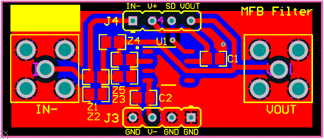
The PCB layout of the top layer of the dual-supply, multiple feedback filter circuit configuration is displayed in Figure 25.
 Figure 25. Dual-Supply, Multiple Feedback Filter Top Layer
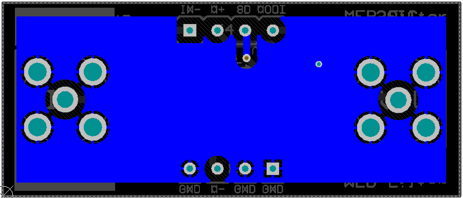
 The PCB layout of the bottom layer of the dual-supply, multiple feedback filter circuit configuration is displayed in Figure 26.
 Figure 26. Dual-Supply, Multiple Feedback Bottom Layer