SBOU192 July 2017
-
DIYAMP-SC70-EVM
- Trademarks
- 1 Introduction
- 2 Hardware Setup
- 3
Schematic and PCB Layout
- 3.1 Schematic PCB Drawing
- 3.2 Single-Supply, Multiple Feedback Filter
- 3.3 Single-Supply, Sallen-Key Filter
- 3.4 Single-Supply, Non-Inverting Amplifier
- 3.5 Single-Supply, Inverting Amplifier
- 3.6 Difference Amplifier
- 3.7 Dual-Supply, Multiple Feedback Filter
- 3.8 Dual-Supply, Sallen-Key Filter
- 3.9 Inverting Comparator
- 3.10 Non-Inverting Comparator
- 3.11 Riso With Dual Feedback
- 3.12 Dual-Supply, Non-Inverting Amplifier
- 3.13 Dual-Supply, Inverting Amplifier
- 4 Connections
- 5 Bill of Materials and Reference
3.6 Difference Amplifier
Figure 21 shows the schematic for the difference amplifier circuit configuration.
 Figure 21. Difference Amplifier Schematic
 The difference amplifier utilizes both inverting and non-inverting inputs and produces an output that is equal to the difference between the inputs. The gain of the difference amplifier is dependent on the ratio of the resistor values selected.
Equation 15 displays the transfer function of the difference amplifier circuit configuration.
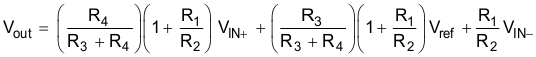
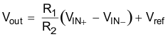
If R1 = R4 and R2 = R3, Equation 15 can be simplified to Equation 16.
Capacitors C1 and C4 provide the option to filter the output of the amplifier. The cutoff frequency of the filter can be calculated using Equation 17.
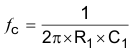
- R1 = R4, R2 = R3, and C1 = C4
where
The PCB layout of the top layer of the difference amplifier circuit configuration is displayed in Figure 22.
 Figure 22. Difference Amplifier Top Layer
 The PCB layout of the bottom layer of the difference amplifier circuit configuration is displayed in Figure 23.
 Figure 23. Difference Amplifier Bottom Layer