SBOU192 July 2017
-
DIYAMP-SC70-EVM
- Trademarks
- 1 Introduction
- 2 Hardware Setup
- 3
Schematic and PCB Layout
- 3.1 Schematic PCB Drawing
- 3.2 Single-Supply, Multiple Feedback Filter
- 3.3 Single-Supply, Sallen-Key Filter
- 3.4 Single-Supply, Non-Inverting Amplifier
- 3.5 Single-Supply, Inverting Amplifier
- 3.6 Difference Amplifier
- 3.7 Dual-Supply, Multiple Feedback Filter
- 3.8 Dual-Supply, Sallen-Key Filter
- 3.9 Inverting Comparator
- 3.10 Non-Inverting Comparator
- 3.11 Riso With Dual Feedback
- 3.12 Dual-Supply, Non-Inverting Amplifier
- 3.13 Dual-Supply, Inverting Amplifier
- 4 Connections
- 5 Bill of Materials and Reference
3.10 Non-Inverting Comparator
Figure 33 shows the schematic for the non-inverting comparator circuit configuration.
 Figure 33. Non-Inverting Comparator Schematic
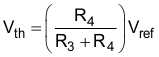
 It is important to note that this circuit layout is meant for SC70 package op amp or push-pull output type comparators. This configuration uses a voltage divider R3 and R4 to set up the threshold voltage. The comparator will compare the input signal (Vin) to the threshold voltage (Vth).
The comparator input signal is applied to the non-inverting input, so the output will have a non-inverted polarity. When Vin > Vth, the output will drive to the positive supply (V+ or logic high). When Vin < Vth, the output will drive to the negative supply (GND or logic low).
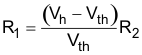
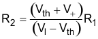
R2 can be populated to implement hysteresis which uses two different threshold voltages to avoid the multiple transitions. The input signal must exceed the upper threshold (VH) to transition high or below the lower threshold (VL) to transition low. Equation 22 and Equation 23 will calculate the value of R1 and R2 for the two desired thresholds.
The PCB layout of the top layer of the non-inverting comparator circuit configuration is displayed in Figure 34.
 Figure 34. Non-inverting Comparator Top Layer
 The PCB layout of the top layer of the non-inverting comparator circuit configuration is displayed in Figure 35.
 Figure 35. Non-Inverting Comparator Bottom Layer