SBAU353 October 2021
3.1 ADC Analog Input Signal Path
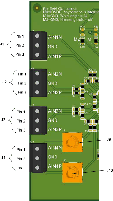
Analog inputs to the EVM can be connected to either the terminal blocks associated with each ADC channel. The screw terminal blocks (J1, J2, J3, and J4) can interface directly with the leads of an external sensor input. There are SMA connectors on channel 4, J9 for AIN4N and J10 for AIN4P, in addition to the terminal blocks that can be utilized as well. Figure 3-1 shows the signal chain used for all four input channels on the EVM and is used to describe the supported input options in Figure 3-1 and Figure 3-2.
An input must not be applied such that the voltage on the input pins of the ADS131A04 exceeds the absolute maximum ratings. For more details, see the ADS131A04 4-Channel, Simultaneously-Sampling, 24-Bit, Delta-Sigma ADC Data Sheet.
R1, R2, and C14 form a differential low-pass filter with a –3-dB cutoff frequency of 169.3 kHz for channel 1. In addition R1 and C15 with R2 and C16 form a common mode low-pass filter with a –3-dB cutoff frequency of 15.9 MHz. The series impedance is kept relatively low in order to maintain adequate total harmonic distortion (THD) performance. Similar differential and common model low pass filters are present on all inputs.
 Figure 3-2 Input Terminal Blocks and
Headers (PCB)
Figure 3-2 Input Terminal Blocks and
Headers (PCB)| Terminal Block | Pin | Function | ADS131A04 Input Pin(s) |
|---|---|---|---|
| J1 | 1 | Channel 0 positive input | AIN0P |
| 2 | EVM ground | AGND and DGND | |
| 3 | Channel 0 negative input | AIN0N | |
| J2 | 1 | Channel 1 positive input | AIN1P |
| 2 | EVM ground | AGND and DGND | |
| 3 | Channel 1 negative input | AIN1N | |
| J3 | 1 | Channel 2 positive input | AIN2P |
| 2 | EVM ground | AGND and DGND | |
| 3 | Channel 2 negative input | AIN2N | |
| J4 | 1 | Channel 3 positive input | AIN3P |
| 2 | EVM ground | AGND and DGND | |
| 3 | Channel 3 negative input | AIN3N |