SBAA531 November 2021 ADS8860 , ADS8862 , ADS8881 , ADS9110 , ADS9224R
- Trademarks
- 1Introduction
-
2
Internal Topology of SAR ADC Model
- 2.1 Sample and Hold
- 2.2 Sample and Hold Timing
- 2.3 Reference Transients
- 2.4 Bandwidth Modeling
- 2.5 Noise Modeling
- 2.6 Reference Droop and Reference Noise Errors
- 2.7 Gain, Offset, and Input Leakage Modeling
- 2.8 Differential input behavior
- 2.9 ESD Protection Diodes and Parasitic Capacitance
- 2.10 Summary of Parameters
- 2.11 Summary of Model Pins
- 3Downloading and Using PSpice® Example Projects From Web
- 4Summary
3.3 Verification of Reference Droop
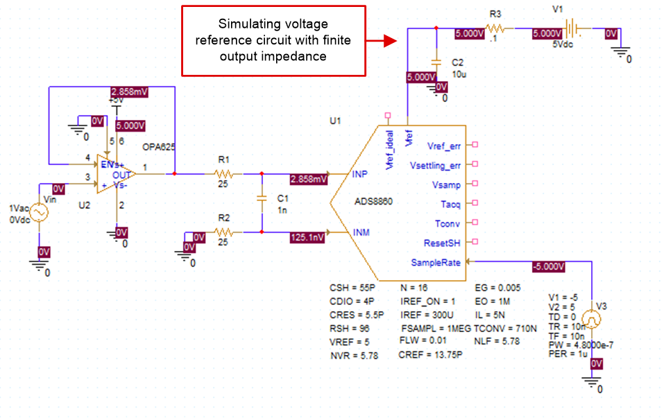
Real-world voltage references have a finite output impedance and bandwidth. These limitations can cause the output voltage of the voltage reference to droop when it is loaded by the transient currents from the ADC reference input pin. Figure 3-10 shows a typical circuit where the impact of the voltage reference limitations can be monitored. The best way to judge the reference settling error is to look at the Vref_err pin. This pin compares the steady state reference input to the transient reference input. The Vsettling_err pin also shows effects of reference droop as it is the total settling error from the sample and hold and reference.
 Figure 3-10 Monitoring Voltage Reference
Settling
Figure 3-10 Monitoring Voltage Reference
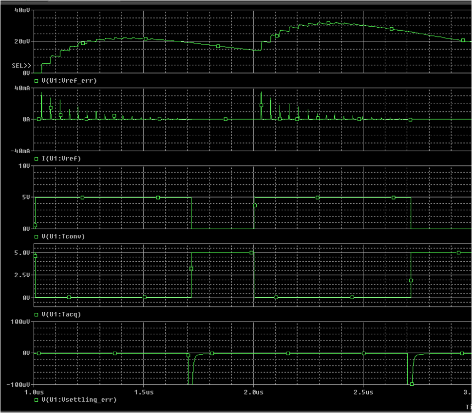
SettlingFigure 3-11 shows the transient simulation results for the voltage reference input on ADS8860. Notice the reference input has transient behavior related to the current transients.
 Figure 3-11 Reference Transient
Simulation