SBAA531 November 2021 ADS8860 , ADS8862 , ADS8881 , ADS9110 , ADS9224R
- Trademarks
- 1Introduction
-
2
Internal Topology of SAR ADC Model
- 2.1 Sample and Hold
- 2.2 Sample and Hold Timing
- 2.3 Reference Transients
- 2.4 Bandwidth Modeling
- 2.5 Noise Modeling
- 2.6 Reference Droop and Reference Noise Errors
- 2.7 Gain, Offset, and Input Leakage Modeling
- 2.8 Differential input behavior
- 2.9 ESD Protection Diodes and Parasitic Capacitance
- 2.10 Summary of Parameters
- 2.11 Summary of Model Pins
- 3Downloading and Using PSpice® Example Projects From Web
- 4Summary
3.1 Selecting the Amplifier and Optimizing the RC Circuit
To get low distortion data acquisition, it is important to select an amplifier with sufficient bandwidth and an external RC circuit that settles quickly. A series of Precision Labs Videos covers this process in great detail. This document quickly summarizes the process. For more information on the subject, see SAR Drive Optimization Video Series.
The first step in designing the drive circuit is selecting the amplifier and choosing a range of values for the RC circuit. The Analog engineer's calculator is a software tool that contains many different utilities to solve common electrical engineering problems. Use the SAR ADC drive tool to determine the amplifier bandwidth and RC filter range for optimal settling on the ADC. Figure 3-2 shows an example using the ADS8860 SAR ADC. The resolution, sample and hold capacitor, full-scale range and acquisition time is entered into the calculator. The calculator output is the minimum amplifier gain bandwidth required, the filter capacitor, and a range of filter resistors. A parameter step operation is used next to find the optimal filter resistor. In this example the bandwidth of the amplifier must be greater than 17.8 MHz, the filter capacitor Cfilt is 1.1 nF, and the filter resistor range is from 8.1 Ω to 65 Ω. There are many amplifiers with a bandwidth exceeding 17.8 MHz. For this example, use the OPA322 which has a bandwidth of 20 MHz. Choosing the amplifier for your application involves looking at all the DC and AC error sources such as offset, bias current, and noise. These tradeoffs are covered in greater detail in the Amplifier Precision Labs video series.
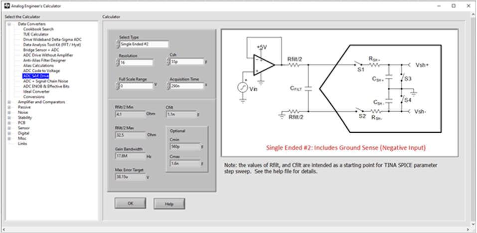 Figure 3-2 Analog Engineer’s
Calculator
Figure 3-2 Analog Engineer’s
CalculatorNext, the filter resistors need to be Parameter Stepped to find the optimal value. There are a number of steps required to do parameter stepping in PSpice. First, place a PARAMETER element. Do this by selecting Place>PSpice Component...>Search from the PSpice menu. Search for PARAM in the search window and place it (See Figure 3-3). Place the PARAMETER element on the schematic near the element you are controlling.
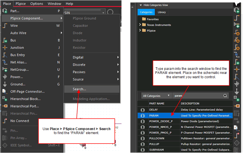 Figure 3-3 Find and Place the PARAMETER
Element
Figure 3-3 Find and Place the PARAMETER
ElementNext, click on the PARAMETER element you just placed to edit it. Press the New Property button. Enter the name for the element you want to control. For example, R_Val to control a resistor. Choose a good value for this element such as 10 for 10 Ω (see Figure 3-4).
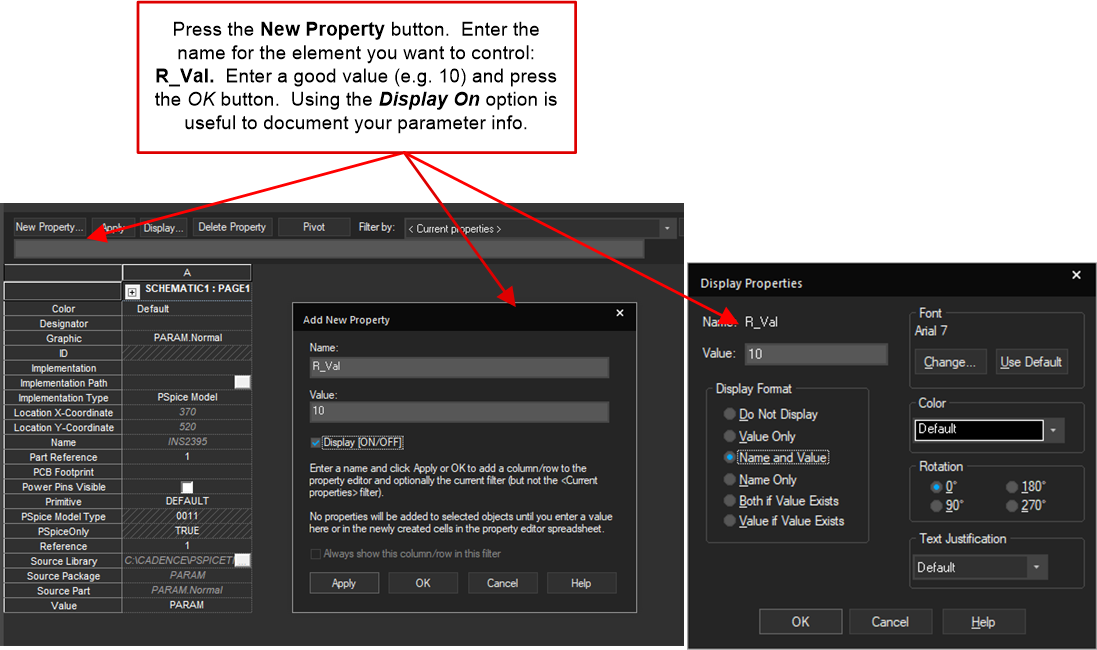 Figure 3-4 Add Property to PARAMETER
Element
Figure 3-4 Add Property to PARAMETER
ElementNext, click on the component you want to edit and change the value to match the value entered in the PARAMETER element. Use braces around the value: {R_Val}. Note that in this example both R4 and R5 are controlled with the same value (see Figure 3-5).
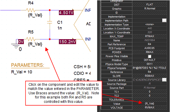 Figure 3-5 Edit the Component Value for
Parameter Stepping
Figure 3-5 Edit the Component Value for
Parameter SteppingThe last step before simulating is to set up the simulation profile. In this case the general settings are set for transient analysis, and the parametric step is set to adjust the filter resistor from 5 Ω to 30 Ω in steps of 5 Ω (see Figure 3-6).
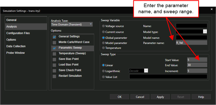 Figure 3-6 Simulation Profile for
Parameter Stepping
Figure 3-6 Simulation Profile for
Parameter SteppingFigure 3-7 shows the settling results. Notice that multiple output curves are present for each measurement. The different curves are all measured with different filter resistor values ranging from 5 Ω to 30 Ω as was selected in the simulation profile. Notice that the settling output response ranges from large overshoot (underdamped) to slow rise time (overdamped). The ideal settling happens with the fastest rise time that does not overshoot (critically damped). Note that for transient simulations, the offset voltage, leakage current, gain, and noise errors are disconnected. Thus, ideally the final settling error is 0 V as the DC error sources are not used in the transient simulation.
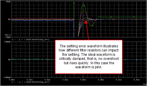 Figure 3-7 Simulation Results for
Parameter Stepping
Figure 3-7 Simulation Results for
Parameter SteppingFigure 3-8 illustrates how you can determine the parameter value that corresponds to the optimal curve. Select the curve, right click, and choose Trace Information. For this example simulation, the optimal settling happened with a 25-Ω filter resistor. It may be useful to first run the parameter step with course limits and then re-run with refined limits for better accuracy.
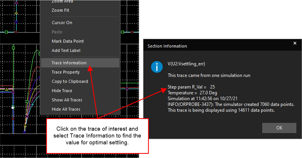 Figure 3-8 Trace Information for
Parameter Stepping