SBAA531 November 2021 ADS8860 , ADS8862 , ADS8881 , ADS9110 , ADS9224R
- Trademarks
- 1Introduction
-
2
Internal Topology of SAR ADC Model
- 2.1 Sample and Hold
- 2.2 Sample and Hold Timing
- 2.3 Reference Transients
- 2.4 Bandwidth Modeling
- 2.5 Noise Modeling
- 2.6 Reference Droop and Reference Noise Errors
- 2.7 Gain, Offset, and Input Leakage Modeling
- 2.8 Differential input behavior
- 2.9 ESD Protection Diodes and Parasitic Capacitance
- 2.10 Summary of Parameters
- 2.11 Summary of Model Pins
- 3Downloading and Using PSpice® Example Projects From Web
- 4Summary
3.4 System Noise Verification
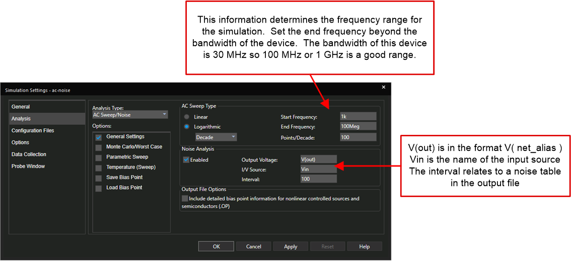
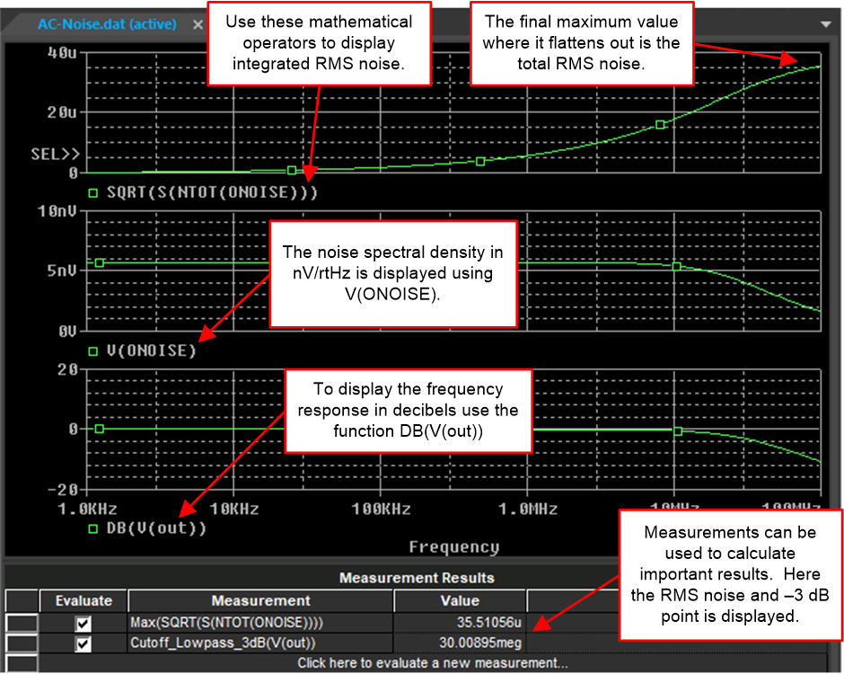
The noise and bandwidth simulations are very useful to determine the overall error of a system due to noise. This simulation includes the noise of the ADC as well as noise from all external components. The noise modeling does not have any impact on the transient simulation and is only measured during an AC-Noise simulation. The total noise for the system is always measured at the Vsamp output on the ADC. Also, this output must be given a Net Alias as the simulation profile uses this to reference the output node. Figure 3-12 shows the simulation profile for the Noise AC-Noise analysis. Figure 3-13 shows the simulation results.
 Figure 3-12 Noise Simulation
Profile
 Figure 3-13 Noise Simulation
Results