SBAA531 November 2021 ADS8860 , ADS8862 , ADS8881 , ADS9110 , ADS9224R
- Trademarks
- 1Introduction
-
2
Internal Topology of SAR ADC Model
- 2.1 Sample and Hold
- 2.2 Sample and Hold Timing
- 2.3 Reference Transients
- 2.4 Bandwidth Modeling
- 2.5 Noise Modeling
- 2.6 Reference Droop and Reference Noise Errors
- 2.7 Gain, Offset, and Input Leakage Modeling
- 2.8 Differential input behavior
- 2.9 ESD Protection Diodes and Parasitic Capacitance
- 2.10 Summary of Parameters
- 2.11 Summary of Model Pins
- 3Downloading and Using PSpice® Example Projects From Web
- 4Summary
3.5 Gain, Offset, and Input Leakage Verification
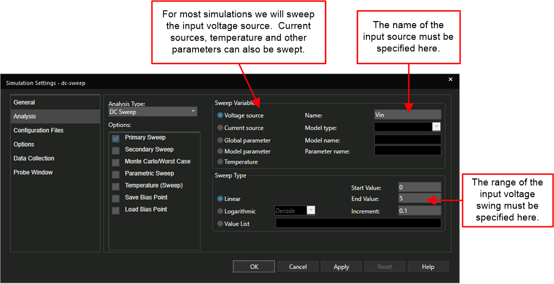
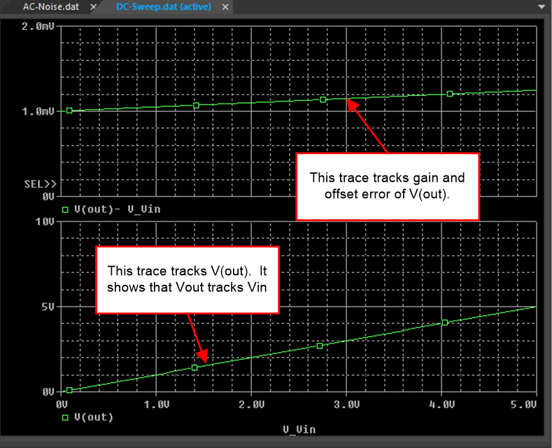
The best way to see the impact of gain error, offset error, and input leakage current is with a DC sweep simulation. The DC sweep generates an input vs output voltage plot. The simulation profile is simple and only requires the input source and range to be specified (see Figure 3-14). Figure 3-15 shows the gain error plot and the output transfer function.
 Figure 3-14 DC Sweep Simulation
Profile
 Figure 3-15 DC Sweep Results