SLUS829G August 2008 – February 2020 UCC2897A
PRODUCTION DATA.
- 1 Features
- 2 Applications
- 3 Description
- 4 Revision History
- 5 Device Options
- 6 Pin Configuration and Functions
- 7 Specifications
-
8 Detailed Description
- 8.1 Overview
- 8.2 Functional Block Diagram
- 8.3 Feature Description
- 8.4 Device Functional Modes
- 9 Application and Implementation
- 10Power Supply Recommendations
- 11Layout
- 12Device and Documentation Support
- 13Mechanical, Packaging, and Orderable Information
封装选项
机械数据 (封装 | 引脚)
散热焊盘机械数据 (封装 | 引脚)
- RGP|20
订购信息
8.3.6 Synchronization
The UCC2897A has a bi-directional synchronization pin. In the stand-alone operation the SYNC pin is driven by the internal oscillator of the UCC2897A which provides an approximately 5-V amplitude square-wave output. This signal synchronizes other PWM controllers or circuits requiring a constant frequency time-base. The synchronization output of the UCC2897A is generated when the internal-timing capacitor reaches the peak value. Therefore, the synchronization waveform does not coincide with the turnon of the main gate-driver output as it is usually implemented in PWM controllers.
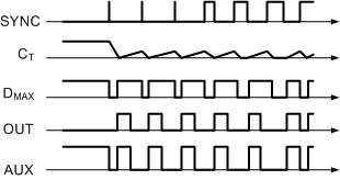
The operation of the oscillator and other relevant waveforms in free-running and synchronized mode are shown in Figure 23.
 Figure 23. A Synchronization Waveform for SYNC Input, P-Channel
 The most critical and unique feature of the oscillator is to limit the maximum-operating duty-cycle of the converter, which is achieved by accurately controlling the charge and discharge intervals of the on-board timing capacitor. The maximum on-time of the OUT pin, which is also the maximum duty-cycle of the active-clamp converter, is limited by the charging-interval of the timing capacitor. While the capacitor is reset to the initial voltage level, OUT is ensured to be off.
When synchronization is used, the rising edge of the signal terminates the charging period and initiates the discharge of the timing capacitor. Once the timing-capacitor voltage reaches the predefined valley-voltage, a new charge period starts automatically. This method of synchronization leaves the charge and discharge slopes of the timing-waveform unaffected thus maintains the maximum duty-cycle of the converter, independent of the operation mode.
Although the synchronization circuit is level sensitive, the actual synchronization event occurs at the rising-edge of the waveform, allowing the synchronizing pulse-width to vary significantly while certain limitations are observed. The minimum pulse-width should be sufficient to ensure reliable triggering of the internal-oscillator circuitry, therefore it is greater than approximately 50 nanoseconds. The other limiting factor is to keep it shorter than Equation 10.
where
- TSYNC is the period of the synchronization frequency
When a pulse wider than that of Equation 10 is connected to the SYNC input, the oscillator is unable to maintain the maximum duty-cycle, originally set by the timing-resistor ratio (RON, ROFF). Furthermore, the timing-capacitor waveform has a flat portion as highlighted by the vertical marker in the timing diagram. During this flat portion of the waveform, both outputs are off, but this state is not compatible with the operation of active-clamp power converters. Therefore, this operating mode is not recommended.
Note that both outputs of the UCC2897A controller are off if the synchronization signal stays continuously high.
When both UCC2897A outputs are synchronized by tying their SYNC pins together, they operate in-phase. It is possible to set different maximum duty-cycle limits for both UCC2897A outputs and still synchronize them by a simple connection between their respective SYNC terminals.