SLUS829G August   2008  – February 2020 UCC2897A

PRODUCTION DATA.  

  1. Features
  2. Applications
  3. Description
    1.     Device Images
      1.      Typical Application Diagram
  4. Revision History
  5. Device Options
  6. Pin Configuration and Functions
    1.     Pin Functions
  7. Specifications
    1. 7.1 Absolute Maximum Ratings
    2. 7.2 ESD Ratings
    3. 7.3 Recommended Operating Conditions
    4. 7.4 Thermal Information
    5. 7.5 Electrical Characteristics
    6. 7.6 Timing Requirements
    7. 7.7 Typical Characteristics
  8. Detailed Description
    1. 8.1 Overview
    2. 8.2 Functional Block Diagram
    3. 8.3 Feature Description
      1. 8.3.1 Detailed Pin Descriptions
        1. 8.3.1.1  RDEL
        2. 8.3.1.2  RON
        3. 8.3.1.3  ROFF
        4. 8.3.1.4  VREF
        5. 8.3.1.5  SYNC
        6. 8.3.1.6  GND
        7. 8.3.1.7  CS
        8. 8.3.1.8  RSLOPE
        9. 8.3.1.9  FB
        10. 8.3.1.10 SS/SD
        11. 8.3.1.11 PGND
        12. 8.3.1.12 AUX
        13. 8.3.1.13 OUT
        14. 8.3.1.14 VDD
        15. 8.3.1.15 LINEUV
        16. 8.3.1.16 VIN
        17. 8.3.1.17 LINEOV
      2. 8.3.2 JFET Control and UVLO
      3. 8.3.3 Line Undervoltage Protection
      4. 8.3.4 Line Overvoltage Protection
      5. 8.3.5 Pulse Skipping
      6. 8.3.6 Synchronization
      7. 8.3.7 Gate Drive Connection
      8. 8.3.8 Bootstrap Biasing
    4. 8.4 Device Functional Modes
  9. Application and Implementation
    1. 9.1 Application Information
    2. 9.2 Typical Application
      1. 9.2.1 Design Requirements
      2. 9.2.2 Detailed Design Procedure
        1. 9.2.2.1 Oscillator
        2. 9.2.2.2 Soft Start
        3. 9.2.2.3 VDD Bypass Requirements
        4. 9.2.2.4 Delay Programming
        5. 9.2.2.5 Input Voltage Monitoring
        6. 9.2.2.6 Current Sense and Slope Compensation
      3. 9.2.3 Application Curves
  10. 10Power Supply Recommendations
  11. 11Layout
    1. 11.1 Layout Guidelines
    2. 11.2 Layout Example
  12. 12Device and Documentation Support
    1. 12.1 Documentation Support
      1. 12.1.1 Related Documentation
    2. 12.2 Receiving Notification of Documentation Updates
    3. 12.3 Community Resources
    4. 12.4 Trademarks
    5. 12.5 Electrostatic Discharge Caution
    6. 12.6 Glossary
  13. 13Mechanical, Packaging, and Orderable Information

封装选项

机械数据 (封装 | 引脚)
散热焊盘机械数据 (封装 | 引脚)
订购信息

Line Overvoltage Protection

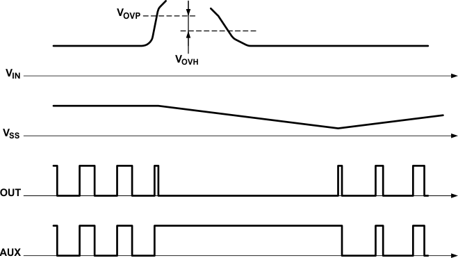
When the line-overvoltage protection is triggered in the UCC2897A controller, the gate-drive signals are immediately disabled. At the same time, the slow discharge of CSS initiates. While the soft-start capacitor discharges the gate-drive signals remain disabled. Once VSS = 0.5 V and the overvoltage disappears from the input of the power supply, operation resumes through a regular soft start of the converter as it is demonstrated in Figure 21. The pulses of OUT and AUX stop if one of three conditions is met:

  1. VDD reaches UVLO off
  2. VSS reaches below 2.5 V
  3. FB voltage is below 2.5 V

UCC2897A line_over_seq_SLUS829.gifFigure 21. Line Overvoltage Sequence, P-Channel