SLUS829G August   2008  – February 2020 UCC2897A

PRODUCTION DATA.  

  1. Features
  2. Applications
  3. Description
    1.     Device Images
      1.      Typical Application Diagram
  4. Revision History
  5. Device Options
  6. Pin Configuration and Functions
    1.     Pin Functions
  7. Specifications
    1. 7.1 Absolute Maximum Ratings
    2. 7.2 ESD Ratings
    3. 7.3 Recommended Operating Conditions
    4. 7.4 Thermal Information
    5. 7.5 Electrical Characteristics
    6. 7.6 Timing Requirements
    7. 7.7 Typical Characteristics
  8. Detailed Description
    1. 8.1 Overview
    2. 8.2 Functional Block Diagram
    3. 8.3 Feature Description
      1. 8.3.1 Detailed Pin Descriptions
        1. 8.3.1.1  RDEL
        2. 8.3.1.2  RON
        3. 8.3.1.3  ROFF
        4. 8.3.1.4  VREF
        5. 8.3.1.5  SYNC
        6. 8.3.1.6  GND
        7. 8.3.1.7  CS
        8. 8.3.1.8  RSLOPE
        9. 8.3.1.9  FB
        10. 8.3.1.10 SS/SD
        11. 8.3.1.11 PGND
        12. 8.3.1.12 AUX
        13. 8.3.1.13 OUT
        14. 8.3.1.14 VDD
        15. 8.3.1.15 LINEUV
        16. 8.3.1.16 VIN
        17. 8.3.1.17 LINEOV
      2. 8.3.2 JFET Control and UVLO
      3. 8.3.3 Line Undervoltage Protection
      4. 8.3.4 Line Overvoltage Protection
      5. 8.3.5 Pulse Skipping
      6. 8.3.6 Synchronization
      7. 8.3.7 Gate Drive Connection
      8. 8.3.8 Bootstrap Biasing
    4. 8.4 Device Functional Modes
  9. Application and Implementation
    1. 9.1 Application Information
    2. 9.2 Typical Application
      1. 9.2.1 Design Requirements
      2. 9.2.2 Detailed Design Procedure
        1. 9.2.2.1 Oscillator
        2. 9.2.2.2 Soft Start
        3. 9.2.2.3 VDD Bypass Requirements
        4. 9.2.2.4 Delay Programming
        5. 9.2.2.5 Input Voltage Monitoring
        6. 9.2.2.6 Current Sense and Slope Compensation
      3. 9.2.3 Application Curves
  10. 10Power Supply Recommendations
  11. 11Layout
    1. 11.1 Layout Guidelines
    2. 11.2 Layout Example
  12. 12Device and Documentation Support
    1. 12.1 Documentation Support
      1. 12.1.1 Related Documentation
    2. 12.2 Receiving Notification of Documentation Updates
    3. 12.3 Community Resources
    4. 12.4 Trademarks
    5. 12.5 Electrostatic Discharge Caution
    6. 12.6 Glossary
  13. 13Mechanical, Packaging, and Orderable Information

封装选项

机械数据 (封装 | 引脚)
散热焊盘机械数据 (封装 | 引脚)
订购信息

Pulse Skipping

During output-load current-transients or light-load conditions most PWM controllers must be able to skip some number of PWM pulses. In an active-clamp topology where the clamp switch is driven complementary to the main switch, the skipping of pulses applies the clamp voltage across the transformer continuously. Since operating conditions might require skipping several switching-cycles on the main transistor, saturating the transformer is very likely if the AUX output remains on.
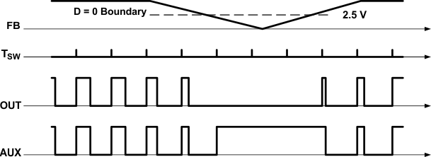
UCC2897A pulse_skip_oper_SLUS829.gifFigure 22. Pulse Skipping Operation, P-Channel

To overcome this problem, the UCC2897A family incorporates pulse skipping for both outputs in the controller. As shown in Figure 22, when a pulse is skipped at the main output (OUT) because the feedback signal demands zero duty-ratio, the corresponding output pulse on the AUX output is omitted as well. This operation prevents reverse saturation of the power transformer and preserves the clamp-capacitor voltage level during pulse-skipping operation.