SLUS829G August 2008 – February 2020 UCC2897A
PRODUCTION DATA.
- 1 Features
- 2 Applications
- 3 Description
- 4 Revision History
- 5 Device Options
- 6 Pin Configuration and Functions
- 7 Specifications
-
8 Detailed Description
- 8.1 Overview
- 8.2 Functional Block Diagram
- 8.3 Feature Description
- 8.4 Device Functional Modes
- 9 Application and Implementation
- 10Power Supply Recommendations
- 11Layout
- 12Device and Documentation Support
- 13Mechanical, Packaging, and Orderable Information
封装选项
机械数据 (封装 | 引脚)
散热焊盘机械数据 (封装 | 引脚)
- RGP|20
订购信息
9.2.2.6 Current Sense and Slope Compensation
The UCC2897A offers onboard user-programmable slope-compensation. The programming of the correct amount of slope compensation is accomplished by the appropriate selection of two external resistors, RF and RSLOPE.
First, the current-sense filter-resistor value (RF) must be calculated based on the desired filtering of the current-sense signal. The filter consists of two components, CF and RF. The CF filter capacitor is connected between the CS pin and the GND pin. While the value of CF is selected freely as the first step of the filter design, the value of CF is minimized to avoid filtering the slope compensation current exiting the CS pin. The recommended range for the filter capacitance is between 50 pF and 270 pF. The value of the filter resistor is calculated from the filter capacitance and the desired filter corner frequency fF.

After RF is defined, RSLOPE is calculated. The amount of slope compensation is defined by the stability requirements of the inner-peak current-loop of the control algorithm and is measured by the number m. When the slope of the applied compensation ramp equals the down-slope of the output-inductor current waveform reflected across the primary-side current-sense resistor (dVL / dt), m = 1. The minimum value of m is 0.5 to prevent current-loop instability. The best current-mode performance is achieved around m = 1. The increase of m moves the control closer to the voltage-mode control operation.
In the UCC2897A controllers, slope compensation is implemented by sourcing a linearly-increasing current at the CS pin. When this current passes through the current-sense filter resistor (RF), the current converts to a slope-compensation ramp which is characterized by (dVS / dt). The (dVS / dt) of the slope-compensation current is defined by RSLOPE according to Equation 27.

where
- 2 V is the peak-to-peak ramp amplitude of the internal oscillator waveform
- 5 is the multiplication factor of the internal current mirror
The voltage equivalent of the compensation ramp (dVS / dt) is obtained easily by multiplying with RF. After introducing the application specific m and (dVL / dt) values, Equation 28 is rearranged for RSLOPE.

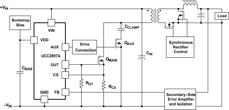
 Figure 29. Active Clamp Forward Converter