SLUS829G August 2008 – February 2020 UCC2897A
PRODUCTION DATA.
- 1 Features
- 2 Applications
- 3 Description
- 4 Revision History
- 5 Device Options
- 6 Pin Configuration and Functions
- 7 Specifications
-
8 Detailed Description
- 8.1 Overview
- 8.2 Functional Block Diagram
- 8.3 Feature Description
- 8.4 Device Functional Modes
- 9 Application and Implementation
- 10Power Supply Recommendations
- 11Layout
- 12Device and Documentation Support
- 13Mechanical, Packaging, and Orderable Information
封装选项
机械数据 (封装 | 引脚)
散热焊盘机械数据 (封装 | 引脚)
- RGP|20
订购信息
8.3.3 Line Undervoltage Protection
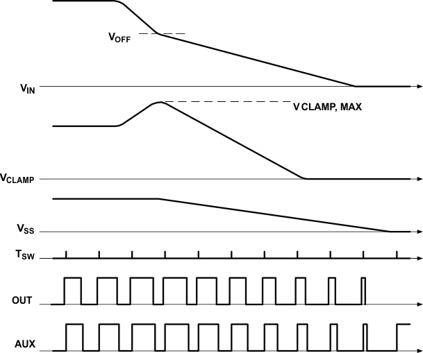
As shown in Figure 20, when the input power-source is removed, the power supply is turned off by the line-undervoltage protection because the bootstrap winding keeps the VDD bias up as long as switching takes place in the power stage. As the input voltage of the power supply decreases gradually toward the line-cutoff voltage, the operating duty cycle of the converter must compensate for the lower input voltage. At minimum input-voltage the duty cycle nears the maximum value (DMAX). Under these conditions the voltage across the clamp capacitor approaches the highest value since the transformer must be reset in a relatively short time. The timing diagram in Figure 20 highlights that in the instance when the converter stops switching the clamp-capacitor voltage might be at the maximum level. Since the only load of the clamp capacitor is the power transformer, this high voltage could linger across the clamp capacitor for a long time when the converter is off. With this high voltage present across the clamp capacitor a soft start would be very dangerous, due to the narrow duty cycle of the main switch and the long on-time of the clamp switch. This could cause the power transformer to saturate during the next soft-start cycle.
 Figure 20. Line Undervoltage Shutdown Waveforms, P-Channel
 To eliminate this potential hazard the UCC2897A controller, discharge the clamp capacitor during power down safely. The OUT and the AUX output continues switching while the soft-start capacitor CSS is being slowly discharged. the function of soft stop is achieved because the AUX pulse-width gradually increases as the clamp voltage decreases, while never applying the high voltage across the transformer for extended period of time.