ZHCSFK9B September 2016 – December 2021 UCC28951-Q1
PRODUCTION DATA
- 1 特性
- 2 应用
- 3 说明
- 4 Revision History
- 5 Pin Configuration and Functions
- 6 Specifications
-
7 Detailed Description
- 7.1 Overview
- 7.2 Functional Block Diagram
- 7.3
Feature Description
- 7.3.1 Start-Up Protection Logic
- 7.3.2 Voltage Reference (VREF)
- 7.3.3 Error Amplifier (EA+, EA–, COMP)
- 7.3.4 Soft-Start and Enable (SS/EN)
- 7.3.5 Light-Load Power Saving Features
- 7.3.6 Adaptive Delay, (Delay Between OUTA and OUTB, OUTC and OUTD (DELAB, DELCD, ADEL))
- 7.3.7 Adaptive Delay (Delay Between OUTA and OUTF, OUTB and OUTE (DELEF, ADELEF)
- 7.3.8 Minimum Pulse (TMIN)
- 7.3.9 Burst Mode
- 7.3.10 Switching Frequency Setting
- 7.3.11 Slope Compensation (RSUM)
- 7.3.12 Dynamic SR ON/OFF Control (DCM Mode)
- 7.3.13 Current Sensing (CS)
- 7.3.14 Cycle-by-Cycle Current Limit Current Protection and Hiccup Mode
- 7.3.15 Synchronization (SYNC)
- 7.3.16 Outputs (OUTA, OUTB, OUTC, OUTD, OUTE, OUTF)
- 7.3.17 Supply Voltage (VDD)
- 7.3.18 Ground (GND)
- 7.4 Device Functional Modes
-
8 Application and Implementation
- 8.1 Application Information
- 8.2
Typical Application
- 8.2.1 Design Requirements
- 8.2.2
Detailed Design Procedure
- 8.2.2.1 Power Loss Budget
- 8.2.2.2 Preliminary Transformer Calculations (T1)
- 8.2.2.3 QA, QB, QC, QD FET Selection
- 8.2.2.4 Selecting LS
- 8.2.2.5 Selecting Diodes DB and DC
- 8.2.2.6 Output Inductor Selection (LOUT)
- 8.2.2.7 Output Capacitance (COUT)
- 8.2.2.8 Select FETs QE and QF
- 8.2.2.9 Input Capacitance (CIN)
- 8.2.2.10 Current Sense Network (CT, RCS, R7, DA)
- 8.2.3 Application Curves
- 9 Power Supply Recommendations
- 10Layout
- 11Device and Documentation Support
7.3.6 Adaptive Delay, (Delay Between OUTA and OUTB, OUTC and OUTD (DELAB, DELCD, ADEL))
The resistor RAB from the DELAB pin, DELAB to GND, along with the resistor divider RAHI from CS pin to ADEL pin and RA from ADEL pin to GND sets the delay TABSET between one of outputs OUTA or OUTB going low and the other output going high Figure 7-1. The total resistance of this resistor divider should be in the range between 10 kΩ and 20 kΩ
 Figure 7-1 Delay Definitions Between OUTA and OUTB, OUTC and OUTD
This delay gradually increases as a function of the CS signal from TABSET1, which is measured at VCS = 1.8 V, to TABSET2, which is measured at the VCS = 0.2 V. This approach ensures there will be no shoot-through current during the high-side and low-side MOSFET switching and optimizes the delay for acheiving ZVS condition over a wide load current range. The ratio between the longest and shortest delays is set by the resistor divider RAHI and RA. The maximum ratio is achieved by tying the CS and ADEL pins together. If ADEL is connected to GND, then the delay is fixed, defined only by the resistor RAB from DELAB to GND. The delay TCDSET1 and TCDSET2 settings and their behaviour for outputs OUTC and OUTD are very similar to the one described for OUTA and OUTB. The difference is that resistor RCD connected between DELCD pin and GND sets the delay TCDSET. The ratio between the longest and shortest delays is set by the resistor divider RAHI and RA.
The delay time TABSET is defined by the following Equation 3.
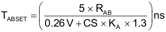
where
- RAB is in kΩ
- CS is the voltage at the CS pin in Volts
- KA is a numerical coefficient in the range from 0 to 1
- the delay time TABSET is in ns and is measured at the IC pins
The same equation is used to define the delay time TCDSET in another leg, except RAB is replaced by RCD (see Equation 4).

where
- RCD is in kΩ
- CS is the voltage at the CS pin in Volts
- KA is a numerical coefficient in the range from 0 to 1
- the delay time TCDSET is in ns and is measured at the IC pins
These equations are empirical and they are approximated from measured data. Thus, there is no unit agreement in the equations. As an example, assume RAB = 15 kΩ, CS = 1 V and KA = 0.5. Then the TABSET is approximately 90 ns.
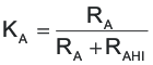
In both Equation 3 and Equation 4, KA is the same and is defined as Equation 5:
KA sets how the delay varies with the CS pin voltage as shown in Figure 7-2 and Figure 7-3.
TI recommends starting by setting KA = 0 and set TABSET and TCDSET relatively large using equations or plots in this data sheet to avoid hard switching or even shoot through current. The delay between outputs A, B and C, D set by resistors RAB and RCD accordingly. Program the optimal delays at light load first. Then by changing KA set the optimal delay for the outputs A, B at maximum current. KA for outputs C, D is the same as for A, B. Usually outputs C, D always have ZVS if sufficient delay is provided.
The allowed resistor range on DELAB and DELCD, RAB and RCD is 13 kΩ to 90 kΩ.
RA and RAHI define the portion of voltage at pin CS applied to the pin ADEL (see Figure 8-3). KA defines how significantly the delay time depends on CS voltage. KA varies from 0, where ADEL pin is shorted to ground (RA = 0) and the delay does not depend on CS voltage, to 1, where ADEL is tied to CS (RAHI = 0). Setting KA, RAB, and RCD provides the ability to maintain optimal ZVS conditions of primary switches over load current because the voltage at CS pin includes the load current reflected to the primary side through the current-sensing circuit. The plots in Figure 7-2 and Figure 7-3 show the delay time settings as a function of CS voltage and KA for two different conditions: RAB = RCD = 13 kΩ (Figure 7-2) and RAB = RCD = 90 kΩ (Figure 7-3).
") Figure 7-2 Delay Time Set TABSET and TCDSET (Over CS Voltage Variation and selected KA for RAB and RCD Equal 13 kΩ)
Figure 7-2 Delay Time Set TABSET and TCDSET (Over CS Voltage Variation and selected KA for RAB and RCD Equal 13 kΩ)") Figure 7-3 Delay Time set TABSET and TCDSET (Over CS Voltage Variation and Selected KA for RAB and RCD Equal 90 kΩ)
Figure 7-3 Delay Time set TABSET and TCDSET (Over CS Voltage Variation and Selected KA for RAB and RCD Equal 90 kΩ)