ZHCSFK9B September 2016 – December 2021 UCC28951-Q1
PRODUCTION DATA
- 1 特性
- 2 应用
- 3 说明
- 4 Revision History
- 5 Pin Configuration and Functions
- 6 Specifications
-
7 Detailed Description
- 7.1 Overview
- 7.2 Functional Block Diagram
- 7.3
Feature Description
- 7.3.1 Start-Up Protection Logic
- 7.3.2 Voltage Reference (VREF)
- 7.3.3 Error Amplifier (EA+, EA–, COMP)
- 7.3.4 Soft-Start and Enable (SS/EN)
- 7.3.5 Light-Load Power Saving Features
- 7.3.6 Adaptive Delay, (Delay Between OUTA and OUTB, OUTC and OUTD (DELAB, DELCD, ADEL))
- 7.3.7 Adaptive Delay (Delay Between OUTA and OUTF, OUTB and OUTE (DELEF, ADELEF)
- 7.3.8 Minimum Pulse (TMIN)
- 7.3.9 Burst Mode
- 7.3.10 Switching Frequency Setting
- 7.3.11 Slope Compensation (RSUM)
- 7.3.12 Dynamic SR ON/OFF Control (DCM Mode)
- 7.3.13 Current Sensing (CS)
- 7.3.14 Cycle-by-Cycle Current Limit Current Protection and Hiccup Mode
- 7.3.15 Synchronization (SYNC)
- 7.3.16 Outputs (OUTA, OUTB, OUTC, OUTD, OUTE, OUTF)
- 7.3.17 Supply Voltage (VDD)
- 7.3.18 Ground (GND)
- 7.4 Device Functional Modes
-
8 Application and Implementation
- 8.1 Application Information
- 8.2
Typical Application
- 8.2.1 Design Requirements
- 8.2.2
Detailed Design Procedure
- 8.2.2.1 Power Loss Budget
- 8.2.2.2 Preliminary Transformer Calculations (T1)
- 8.2.2.3 QA, QB, QC, QD FET Selection
- 8.2.2.4 Selecting LS
- 8.2.2.5 Selecting Diodes DB and DC
- 8.2.2.6 Output Inductor Selection (LOUT)
- 8.2.2.7 Output Capacitance (COUT)
- 8.2.2.8 Select FETs QE and QF
- 8.2.2.9 Input Capacitance (CIN)
- 8.2.2.10 Current Sense Network (CT, RCS, R7, DA)
- 8.2.3 Application Curves
- 9 Power Supply Recommendations
- 10Layout
- 11Device and Documentation Support
8.2.2.2 Preliminary Transformer Calculations (T1)
Transformer turns ratio (a1) is:

Estimate FET voltage drop (VRDSON) as: VRDSON = 0.3 V
Select transformer turns based on 70% duty cycle (DMAX) at minimum specified input voltage. This will give some room for dropout if a PFC front end is used (see Equation 24 and Equation 25).
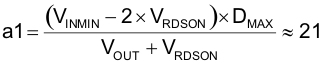
Turn the ratio and round is to the nearest whole turn: a1 = 21
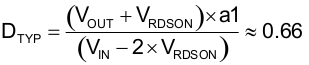
Calculate the typical duty cycle (DTYP) based on average input voltage in Equation 26.
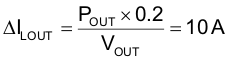
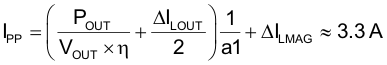
Output inductor peak-to-peak ripple current is set to 20% of the output current using Equation 27.
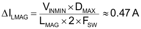
Take care in selecting the correct amount of magnetizing inductance (LMAG). Equation 28 calculates the minimum magnetizing inductance of the primary of the transformer (T1) to ensure the converter operates in current-mode control. As LMAG reduces, the increasing magnetizing current becomes an increasing proportion of the signal at the CS pin. If the magnetizing current increases enough, it can swamp out the current sense signal across RCS and the converter will operate increasingly as if it were in voltage mode control rather than current mode.
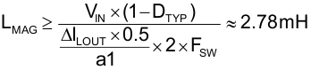
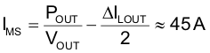
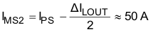
Figure 8-4 shows T1 primary current (IPRIMARY) and synchronous rectifiers QE (IQE) and QF (IQF) currents with respect to the synchronous rectifier gate drive currents. IQE and IQF are the same as the secondary winding currents of T1. Variable D is the duty cycle of the converter.
 Figure 8-4 T1
Primary and QE and QF FET Currents
Figure 8-4 T1
Primary and QE and QF FET CurrentsCalculate T1 secondary RMS current (ISRMS) in Equation 29 through Equation 31:
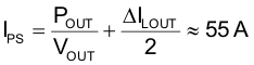
Secondary RMS current (ISRMS1) when energy is being delivered to the secondary (see Equation 32):
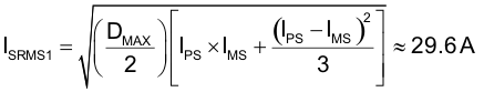
Secondary RMS current (ISRMS2) when current is circulating through the transformer when QE and QF are both on (see Equation 33).
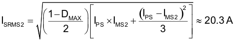
Secondary RMS current (ISRMS3) caused by the negative current in the opposing winding during freewheeling period calculated in Equation 34. Refer to Figure 8-4.
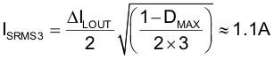
Total secondary RMS current (ISRMS) is calculated in Equation 35:

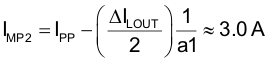
Calculate T1 Primary RMS Current (IPRMS) using Equation 36 through Equation 40:
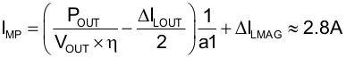
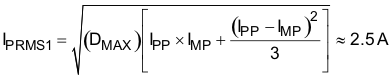
T1 Primary RMS (IPRMS1) current when energy is being delivered to the secondary (see Equation 41).
T1 Primary RMS (IPRMS2) current when the converter is free wheeling. This is calculated in Equation 42:
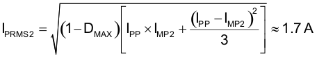
The total T1 primary RMS current (IPRMS) is calculated using Equation 43:

For this design, a Vitec™ transformer was selected for part number 75PR8107 with the following specifications:
- a1 = 21
- LMAG = 2.8 mH
- measured leakage inductance on the Primary (LLK) is 4 µH
- transformer Primary DC resistance (DCRP) is 0.215 Ω
- transformer Secondary DC resistance (DCRS) is 0.58 mΩ
- estimated transformer core losses (PT1) calculated in Equation 44 are twice the copper loss (which is an estimate and the total losses may vary based on magnetic design)

Calculate remaining power budget using Equation 45: