ZHCSD93A january 2015 – december 2020 UCC28700-Q1
PRODUCTION DATA
- 1
- 1 特性
- 2 应用
- 3 说明
- 4 Revision History
- 5 Pin Configuration and Functions
- 6 Specifications
- 7 Detailed Description
-
8 Applications and Implementation
- 8.1 Application Information
- 8.2
Typical Application
- 8.2.1 Design Requirements
- 8.2.2
Detailed Design Procedure
- 8.2.2.1 Transformer Parameter Verification
- 8.2.2.2 Output Capacitance
- 8.2.2.3 VDD Capacitance, CDD
- 8.2.2.4 VDD Start-Up Resistance, RSTR
- 8.2.2.5 VS Resistor Divider, Line Compensation, and Cable Compensation
- 8.2.2.6 Input Bulk Capacitance and Minimum Bulk Voltage
- 8.2.2.7 Transformer Turns Ratio, Inductance, Primary-Peak Current
- 8.2.2.8 Standby Power Estimate
- 8.2.3 Application Curves
- 9 Power Supply Recommendations
- 10Layout
-
11Device and Documentation Support
- 11.1
Device Support
- 11.1.1
Device Nomenclature
- 11.1.1.1 Capacitance Terms in Farads
- 11.1.1.2 Duty Cycle Terms
- 11.1.1.3 Frequency Terms in Hertz
- 11.1.1.4 Current Terms in Amperes
- 11.1.1.5 Current and Voltage Scaling Terms
- 11.1.1.6 Transformer Terms
- 11.1.1.7 Power Terms in Watts
- 11.1.1.8 Resistance Terms in Ω
- 11.1.1.9 Timing Terms in Seconds
- 11.1.1.10 Voltage Terms in Volts
- 11.1.1.11 AC Voltage Terms in VRMS
- 11.1.1.12 Efficiency Terms
- 11.1.1
Device Nomenclature
- 11.2 Documentation Support
- 11.3 Trademarks
- 11.1
Device Support
- Mechanical, Packaging, and Orderable Information
7.3.1.6 CBC (Cable Compensation)
The cable compensation pin is connected to a resistor to ground to program the amount of output voltage compensation to offset cable resistance. The cable compensation block provides a 0-V to 3-V voltage level on the CBC pin corresponding to 0 to IOCC output current. The resistance selected on the CBC pin programs a current mirror that is summed into the VS feedback divider therefore increasing the output voltage as IOUT increases. There is an internal series resistance of 28 kΩ to the CBC pin which sets a maximum cable compensation of a 5-V output to 400 mV when CBC is shorted to ground. The CBC resistance value can be determined by the equation below.
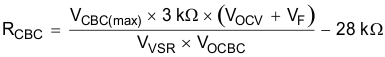
where
- VO is the output voltage,
- VF is the diode forward voltage,
- VOCBC is the target cable compensation voltage at the output terminals,
- VCBC(max) is the maximum voltage at the cable compensation pin at the maximum converter output current (see the Section 6.5 table),
- VVSR is the CV regulating level at the VS input (see the Section 6.5 table).