ZHCSD93A january 2015 – december 2020 UCC28700-Q1
PRODUCTION DATA
- 1
- 1 特性
- 2 应用
- 3 说明
- 4 Revision History
- 5 Pin Configuration and Functions
- 6 Specifications
- 7 Detailed Description
-
8 Applications and Implementation
- 8.1 Application Information
- 8.2
Typical Application
- 8.2.1 Design Requirements
- 8.2.2
Detailed Design Procedure
- 8.2.2.1 Transformer Parameter Verification
- 8.2.2.2 Output Capacitance
- 8.2.2.3 VDD Capacitance, CDD
- 8.2.2.4 VDD Start-Up Resistance, RSTR
- 8.2.2.5 VS Resistor Divider, Line Compensation, and Cable Compensation
- 8.2.2.6 Input Bulk Capacitance and Minimum Bulk Voltage
- 8.2.2.7 Transformer Turns Ratio, Inductance, Primary-Peak Current
- 8.2.2.8 Standby Power Estimate
- 8.2.3 Application Curves
- 9 Power Supply Recommendations
- 10Layout
-
11Device and Documentation Support
- 11.1
Device Support
- 11.1.1
Device Nomenclature
- 11.1.1.1 Capacitance Terms in Farads
- 11.1.1.2 Duty Cycle Terms
- 11.1.1.3 Frequency Terms in Hertz
- 11.1.1.4 Current Terms in Amperes
- 11.1.1.5 Current and Voltage Scaling Terms
- 11.1.1.6 Transformer Terms
- 11.1.1.7 Power Terms in Watts
- 11.1.1.8 Resistance Terms in Ω
- 11.1.1.9 Timing Terms in Seconds
- 11.1.1.10 Voltage Terms in Volts
- 11.1.1.11 AC Voltage Terms in VRMS
- 11.1.1.12 Efficiency Terms
- 11.1.1
Device Nomenclature
- 11.2 Documentation Support
- 11.3 Trademarks
- 11.1
Device Support
- Mechanical, Packaging, and Orderable Information
7.3.1.5 CS (Current Sense)
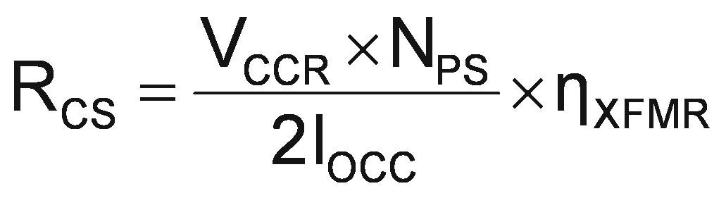
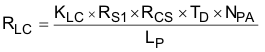
The current-sense pin is connected through a series resistor (RLC) to the current-sense resistor (RCS). The current-sense threshold is 0.75 V for IPP(max) and 0.25 V for IPP(min). The series resistor RLC provides the function of feed-forward line compensation to eliminate change in IPP due to change in di/dt and the propagation delay of the internal comparator and MOSFET turn-off time. There is an internal leading-edge blanking time of 235 ns to eliminate sensitivity to the MOSFET turn-on current spike. It should not be necessary to place a bypass capacitor on the CS pin. The value of RCS is determined by the target output current in constant-current (CC) regulation. The values of RCS and RLC can be determined by the equations below. The term ηXFMR is intended to account for the energy stored in the transformer but not delivered to the secondary. This includes transformer resistance and core loss, bias power, and primary-to-secondary leakage ratio.
Example: With a transformer core and winding loss of 5%, primary-to-secondary leakage inductance of 3.5%, and bias power to output power ratio of 1.5%. The ηXFMR value is approximately: 1 - 0.05 - 0.035 - 0.015 = 0.9.
where
- VCCR is a current regulation constant (see the Section 6.5 table),
- NPS is the transformer primary-to-secondary turns ratio (a ratio of 13 to 15 is recommended for 5-V output),
- IOCC is the target output current in constant-current regulation,
- ηXFMR is the transformer efficiency.
where
- RS1 is the VS pin high-side resistor value,
- RCS is the current-sense resistor value,
- TD is the current-sense delay including MOSFET turn-off delay, add ~50 ns to MOSFET delay,
- NPA is the transformer primary-to-auxiliary turns ratio,
- LP is the transformer primary inductance,
- KLC is a current-scaling constant (see the Section 6.5 table).