ZHCSD93A january 2015 – december 2020 UCC28700-Q1
PRODUCTION DATA
- 1
- 1 特性
- 2 应用
- 3 说明
- 4 Revision History
- 5 Pin Configuration and Functions
- 6 Specifications
- 7 Detailed Description
-
8 Applications and Implementation
- 8.1 Application Information
- 8.2
Typical Application
- 8.2.1 Design Requirements
- 8.2.2
Detailed Design Procedure
- 8.2.2.1 Transformer Parameter Verification
- 8.2.2.2 Output Capacitance
- 8.2.2.3 VDD Capacitance, CDD
- 8.2.2.4 VDD Start-Up Resistance, RSTR
- 8.2.2.5 VS Resistor Divider, Line Compensation, and Cable Compensation
- 8.2.2.6 Input Bulk Capacitance and Minimum Bulk Voltage
- 8.2.2.7 Transformer Turns Ratio, Inductance, Primary-Peak Current
- 8.2.2.8 Standby Power Estimate
- 8.2.3 Application Curves
- 9 Power Supply Recommendations
- 10Layout
-
11Device and Documentation Support
- 11.1
Device Support
- 11.1.1
Device Nomenclature
- 11.1.1.1 Capacitance Terms in Farads
- 11.1.1.2 Duty Cycle Terms
- 11.1.1.3 Frequency Terms in Hertz
- 11.1.1.4 Current Terms in Amperes
- 11.1.1.5 Current and Voltage Scaling Terms
- 11.1.1.6 Transformer Terms
- 11.1.1.7 Power Terms in Watts
- 11.1.1.8 Resistance Terms in Ω
- 11.1.1.9 Timing Terms in Seconds
- 11.1.1.10 Voltage Terms in Volts
- 11.1.1.11 AC Voltage Terms in VRMS
- 11.1.1.12 Efficiency Terms
- 11.1.1
Device Nomenclature
- 11.2 Documentation Support
- 11.3 Trademarks
- 11.1
Device Support
- Mechanical, Packaging, and Orderable Information
8.2.2.2 Output Capacitance
The output capacitance value is typically determined by the transient response requirement from no-load. For example, in some USB charger applications there is a requirement to maintain a minimum VO of 4.1 V with a load-step transient of 0 mA to 500 mA . The equation below assumes that the switching frequency can be at the UCC28700-Q1 minimum of fSW(min).
Equation 11. 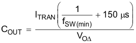
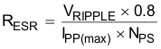
Another consideration of the output capacitor(s) is the ripple voltage requirement which is reviewed based on secondary peak current and ESR. A margin of 20% is added to the capacitor ESR requirement in the equation below.
Equation 12.