ZHCSD93A january 2015 – december 2020 UCC28700-Q1
PRODUCTION DATA
- 1
- 1 特性
- 2 应用
- 3 说明
- 4 Revision History
- 5 Pin Configuration and Functions
- 6 Specifications
- 7 Detailed Description
-
8 Applications and Implementation
- 8.1 Application Information
- 8.2
Typical Application
- 8.2.1 Design Requirements
- 8.2.2
Detailed Design Procedure
- 8.2.2.1 Transformer Parameter Verification
- 8.2.2.2 Output Capacitance
- 8.2.2.3 VDD Capacitance, CDD
- 8.2.2.4 VDD Start-Up Resistance, RSTR
- 8.2.2.5 VS Resistor Divider, Line Compensation, and Cable Compensation
- 8.2.2.6 Input Bulk Capacitance and Minimum Bulk Voltage
- 8.2.2.7 Transformer Turns Ratio, Inductance, Primary-Peak Current
- 8.2.2.8 Standby Power Estimate
- 8.2.3 Application Curves
- 9 Power Supply Recommendations
- 10Layout
-
11Device and Documentation Support
- 11.1
Device Support
- 11.1.1
Device Nomenclature
- 11.1.1.1 Capacitance Terms in Farads
- 11.1.1.2 Duty Cycle Terms
- 11.1.1.3 Frequency Terms in Hertz
- 11.1.1.4 Current Terms in Amperes
- 11.1.1.5 Current and Voltage Scaling Terms
- 11.1.1.6 Transformer Terms
- 11.1.1.7 Power Terms in Watts
- 11.1.1.8 Resistance Terms in Ω
- 11.1.1.9 Timing Terms in Seconds
- 11.1.1.10 Voltage Terms in Volts
- 11.1.1.11 AC Voltage Terms in VRMS
- 11.1.1.12 Efficiency Terms
- 11.1.1
Device Nomenclature
- 11.2 Documentation Support
- 11.3 Trademarks
- 11.1
Device Support
- Mechanical, Packaging, and Orderable Information
8.2.2.7 Transformer Turns Ratio, Inductance, Primary-Peak Current
The maximum primary-to-secondary turns ratio can be determined by the target maximum switching frequency at full load, the minimum input capacitor bulk voltage, and the estimated DCM quasi-resonant time.
Initially determine the maximum available total duty cycle of the on time and secondary conduction time based on target switching frequency and DCM resonant time. For DCM resonant time, assume 500 kHz if you do not have an estimate from previous designs. For the transition mode operation limit, the period required from the end of secondary current conduction to the first valley of the VDS voltage is ½ of the DCM resonant period, or 1 µs assuming 500-kHz resonant frequency. DMAX can be determined using the equation below.
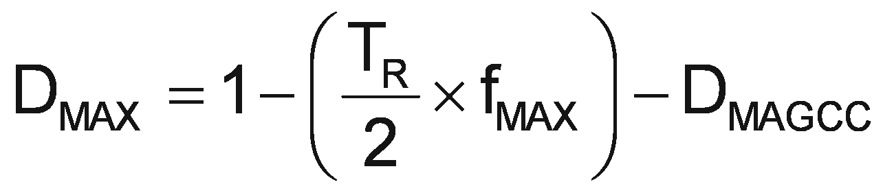
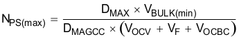
Once DMAX is known, the maximum turns ratio of the primary to secondary can be determined with the equation below. DMAGCC is defined as the secondary diode conduction duty cycle during constant-current, CC, operation. It is set internally by the UCC28700-Q1 at 0.425. The total voltage on the secondary winding needs to be determined; which is the sum of VOCV, the secondary rectifier VF, and the cable compensation voltage (VOCBC). For the 5-V USB charger applications, a turns ratio range of 13 to 15 is typically used.
Once an optimum turns ratio is determined from a detailed transformer design, use this ratio for the following parameters.
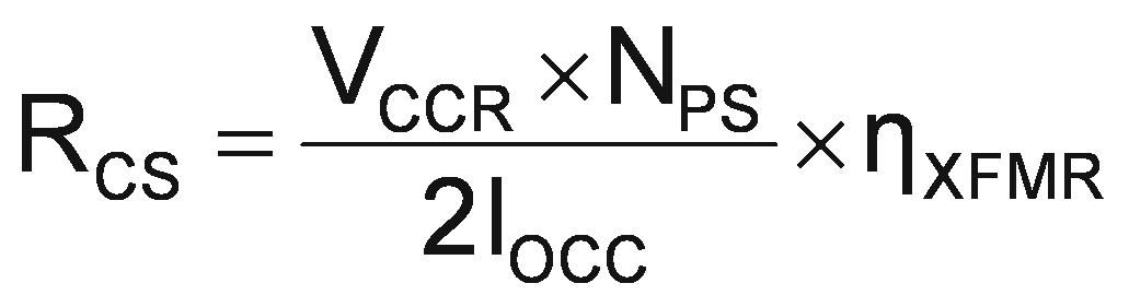
The UCC28700-Q1 controller constant-current regulation is achieved by maintaining a maximum DMAG duty cycle of 0.425 at the maximum primary current setting. The transformer turns ratio and constant-current regulating voltage determine the current sense resistor for a target constant current.
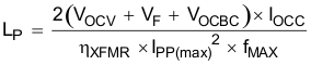
Since not all of the energy stored in the transformer is transferred to the secondary, a transformer efficiency term is included. This efficiency number includes the core and winding losses, leakage inductance ratio, and bias power ratio to rated output power. For a 5-V, 1-A charger example, bias power of 1.5% is a good estimate. An overall transformer efficiency of 0.9 is a good estimate to include 3.5% leakage inductance, 5% core and winding loss, and 1.5% bias power.
The primary transformer inductance can be calculated using the standard energy storage equation for flyback transformers. Primary current, maximum switching frequency and output and transformer power losses are included in the equation below. Initially determine transformer primary current.
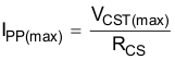
Primary current is simply the maximum current sense threshold divided by the current sense resistance.
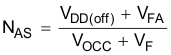
The secondary winding to auxiliary winding transformer turns ratio (NAS) is determined by the lowest target operating output voltage in constant-current regulation and the VDD UVLO of the UCC28700-Q1. There is additional energy supplied to VDD from the transformer leakage inductance energy which allows a lower turns ratio to be used in many designs.