SLUS168F April 1999 – July 2025 UCC2808-1 , UCC2808-2 , UCC3808-1 , UCC3808-2
PRODUCTION DATA
4 Pin Configuration and Functions
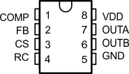
 Figure 4-1 D Package, 8-Pin SOIC (Top
View)
Figure 4-1 D Package, 8-Pin SOIC (Top
View)Table 4-1 Pin Functions
| PIN | Type(1) | DESCRIPTION | |
|---|---|---|---|
| NAME | NO. | ||
| COMP | 1 | I/O | Output of the error amplifier and the input of the PWM comparator. |
| CS | 3 | I | Input to the PWM, peak current, and overcurrent comparators. |
| FB | 2 | I | Inverting input to the error amplifier. |
| GND | 5 | — | Reference ground and power ground for all functions. |
| OUTA | 7 | O | Alternating high current output stage. |
| OUTB | 6 | O | Alternating high current output stage. |
| RC | 4 | I | Oscillator programming pin. |
| VDD | 8 | — | Power input connection for this device. |
(1) I=Input; O=Output; I/O= Input or Output