ZHCS779C March 2012 – July 2025 UCC28070 , UCC28070A
PRODUCTION DATA
- 1
- 1 特性
- 2 应用
- 3 说明
- 4 Pin Configuration and Functions
- 5 Specifications
-
6 Detailed Description
- 6.1 Overview
- 6.2 Functional Block Diagram
- 6.3
Feature Description
- 6.3.1 Interleaving
- 6.3.2 Programming the PWM Frequency and Maximum Duty-Cycle Clamp
- 6.3.3 Frequency Dithering (Magnitude and Rate)
- 6.3.4 External Clock Synchronization
- 6.3.5 Multi-phase Operation
- 6.3.6 VSENSE and VINAC Resistor Configuration
- 6.3.7 VSENSE and VINAC Open-Circuit Protection
- 6.3.8 Current Synthesizer
- 6.3.9 Programmable Peak Current Limit
- 6.3.10 Linear Multiplier and Quantized Voltage Feed Forward
- 6.3.11 Enhanced Transient Response (VA Slew-Rate Correction)
- 6.3.12 Bias Voltages (VCC and VREF)
- 6.3.13 PFC Enable and Disable
- 6.3.14 Adaptive Soft-Start
- 6.3.15 PFC Start-Up Hold Off
- 6.3.16 Output Overvoltage Protection (OVP)
- 6.3.17 Zero-Power Detection
- 6.3.18 Thermal Shutdown
- 6.3.19 Current Loop Compensation
- 6.3.20 Voltage Loop Compensation
- 6.4 Device Functional Modes
-
7 Application and Implementation
- 7.1 Application Information
- 7.2
Typical Application
- 7.2.1 Design Requirements
- 7.2.2
Detailed Design Procedure
- 7.2.2.1 Output Current Calculation
- 7.2.2.2 Bridge Rectifier
- 7.2.2.3 PFC Inductor (L1 and L2)
- 7.2.2.4 PFC MOSFETs (M1 and M2)
- 7.2.2.5 PFC Diode
- 7.2.2.6 PFC Output Capacitor
- 7.2.2.7 Current-Loop Feedback Configuration (Sizing of the Current-Transformer Turns-Ratio NCT and Current-Sense Resistor RS)
- 7.2.2.8 Current-Sense Offset and PWM Ramp for Improved Noise Immunity
- 7.2.3 Application Curves
- 7.3 Power Supply Recommendations
- 7.4 Layout
- 8 器件和文档支持
- 9 Revision History
- 10Mechanical, Packaging, and Orderable Information
6.3.6 VSENSE and VINAC Resistor Configuration
The primary purpose of the VSENSE input is to provide the voltage feedback from the output to the voltage control loop. Thus, a traditional resistor-divider network must be sized and connected between the output capacitor and the VSENSE pin to set the desired output voltage based on the 3V regulation voltage on VSENSE.
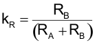
A unique aspect of the UCC28070A is the need to place the same resistor-divider network on the VIN side of the inductor to the VINAC pin. This provides the scaled input voltage monitoring needed for the linear multiplier and current synthesizer circuitry. It is not required that the actual resistance of the VINAC network be identical to the VSENSE network, but it is necessary that the attenuation (kR) of the two divider networks be equivalent for proper PFC operation.
In noisy environments, it may be beneficial for small filter capacitors to be applied to the VSENSE and VINAC inputs to avoid the destabilizing effects of excessive noise on these inputs. If applied, the RC time-constant must not exceed 100μs on the VSENSE input to avoid significant delay in the output transient response. The RC time-constant must also not exceed 100μs on the VINAC input to avoid degrading of the wave-shape zero-crossings. Usually, a time constant of 3 / fPWM is adequate to filter out typical noise on VSENSE and VINAC. Some design and test iteration may be required to find the optimal amount of filtering required in a particular application.