ZHCSNM5C november 2020 – august 2023 UCC25800-Q1
PRODUCTION DATA
- 1
- 1 特性
- 2 应用
- 3 说明
- 4 Revision History
- 5 Device Comparison Table
- 6 Pin Configuration and Functions
- 7 Specifications
- 8 Detailed Description
- 9 Application and Implementation
- 10Power Supply Recommendations
- 11Layout
- 12Device and Documentation Support
- 13Mechanical, Packaging, and Orderable Information
8.3.5.1.2 Output Power Capability
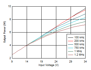
Figure 8-15 shows the output power capability of the UCC25800-Q1 transformer driver at different input voltages and switching frequencies with its highest OCP set-point (IOCP = IOCP1max = 1 A), based on an input-output efficiency of 90%. There are two limiting factors on the power handling capability of the transformer driver; the OCP1 threshold and the thermal stress.
OCP1 serves as an over-power limit rather than over current protection since it has a 2.1-ms timer. Given its maximum value is 1 A and considering the sinusoidal current shaped, transformer driver limits its maximum output power proportionally to the input voltage. In Figure 8-15, the 100-kHz line is approximately the OCP1 limit.
The thermal limitation is to prevent the junction temperature of the transformer driver from becoming too high. Assuming its loss is only the IC bias consumption and the MOSFET conduction loss, at 125°C ambient temperature and 90% efficiency, the maximum output power creates the loss to make the junction temperature reach 150°C. Figure 8-15 shows that with higher the switching frequency, the IC power consumption increases and the maximum power capability decreases.
The power handling capability can be increased by increasing the input voltage or lowering the switching frequency, but it cannot exceed the OCP1 limit.
 Figure 8-15 Power rating curves