ZHCSNM5C november 2020 – august 2023 UCC25800-Q1
PRODUCTION DATA
- 1
- 1 特性
- 2 应用
- 3 说明
- 4 Revision History
- 5 Device Comparison Table
- 6 Pin Configuration and Functions
- 7 Specifications
- 8 Detailed Description
- 9 Application and Implementation
- 10Power Supply Recommendations
- 11Layout
- 12Device and Documentation Support
- 13Mechanical, Packaging, and Orderable Information
9.2.1 LLC Converter Operation Principle
Different than the traditional PWM converters, LLC converters adjust the output voltage through varying the switching frequency. It is often called a PFM (pulse frequency modulation) converter. As shown in Figure 9-3, the LLC converter has three resonant elements, the resonant inductor (Lr), the magnetizing inductor (Lm), and the resonant capacitor (Cr). In the isolated bias supply design, the transformer leakage inductor, and the magnetizing inductor can be used as part of the resonant circuit. In this case, the only external resonant component is the resonant capacitor.
 Figure 9-3 LLC Converter
At the resonant switching frequency (series resonant frequency of Lr and Cr), the impedance of the resonant tank (Lr and Cr) is equal to zero. The input and output voltage are virtually connected together through the transformer. Therefore, the gain of the converter is equal to the transformer turns ratio, as shown in Equation 8.
In this equation, the ½ comes from the half-bridge architecture that the transformer primary side only sees half of the input voltage.
UCC25800-Q1 transformer driver controls the LLC converter to operate at a fixed switching frequency very close to the resonant frequency, to create an output voltage proportional to the input voltage, through a transformer turns-ratio. Depending on the location of the resonant capacitor, the LLC converter can be configured as primary-side resonant (as shown in Figure 9-3), or secondary-side resonant (as shown in Figure 9-4). When the resonant capacitor is moved to the secondary side, the magnetizing inductor no longer affects the converter gain. Therefore, the converter is less sensitive to the switching frequency and resonant component tolerances. The secondary-side resonant is more suitable for the open-loop LLC converter and it is a preferred configuration for transformer driver.
 Figure 9-4 Secondary side resonant LLC
converter
Figure 9-4 Secondary side resonant LLC
converterFurthermore, the secondary-side full-wave rectifier can be replaced with a voltage-doubler rectifier. Together with splitting the resonant capacitor into two, as shown in Figure 9-5, the converter configuration becomes simpler and fewer diodes are used. In this case, the transformer primary side sees half of the input voltage and the transformer secondary side sees half of the output voltage. The converter voltage gain becomes purely the transformer turns-ratio, as shown in Equation 9.
 Figure 9-5 Secondary side resonant LLC converter with voltage doubler rectifier
The LLC operation waveforms are shown in Figure 9-6, when switching frequency is equal to the resonant frequency or below the resonant frequency.
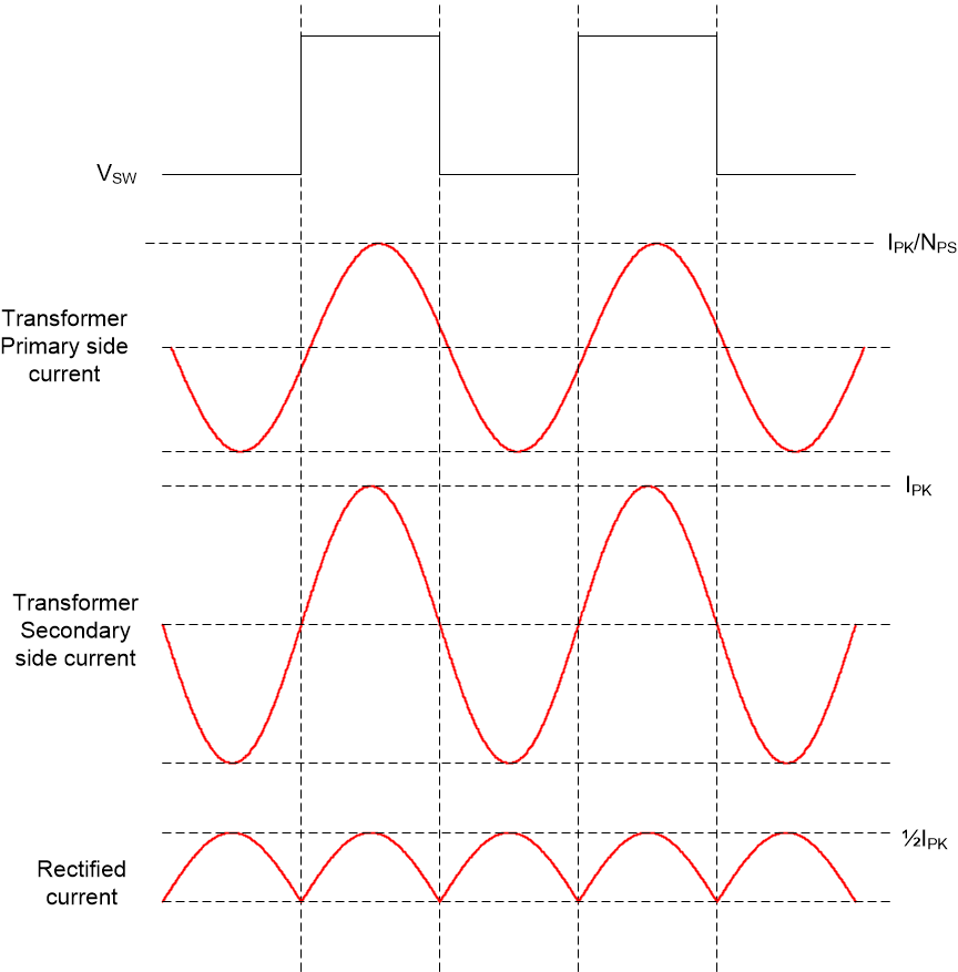 (a) Switching frequency equal to resonant frequency |
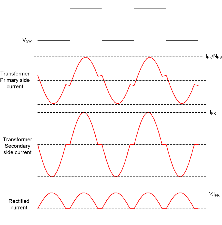 (b) Switching frequency below resonant frequency |