ZHCSJY8E june 2019 – february 2021 UCC256402 , UCC256403 , UCC256404
PRODUCTION DATA
- 1 特性
- 2 应用
- 3 说明
- 4 Revision History
- 5 Pin Configuration and Functions
- 6 Specifications
-
7 Detailed Description
- 7.1 Overview
- 7.2 Functional Block Diagram
- 7.3 Feature Description
- 7.4
Device Functional Modes
- 7.4.1 High Voltage Start-Up
- 7.4.2 X-Capacitor Discharge
- 7.4.3 Burst Mode Control
- 7.4.4
System State Machine
-
Application and Implementation
- 8.1 Application Information
- 8.2
Typical Application
- 8.2.1 Design Requirements
- 8.2.2
Detailed Design Procedure
- 8.2.2.1 LLC Power Stage Requirements
- 8.2.2.2 LLC Gain Range
- 8.2.2.3 Select Ln and Qe
- 8.2.2.4 Determine Equivalent Load Resistance
- 8.2.2.5 Determine Component Parameters for LLC Resonant Circuit
- 8.2.2.6 LLC Primary-Side Currents
- 8.2.2.7 LLC Secondary-Side Currents
- 8.2.2.8 LLC Transformer
- 8.2.2.9 LLC Resonant Inductor
- 8.2.2.10 LLC Resonant Capacitor
- 8.2.2.11 LLC Primary-Side MOSFETs
- 8.2.2.12 LLC Rectifier Diodes
- 8.2.2.13 LLC Output Capacitors
- 8.2.2.14 HV Pin Series Resistors
- 8.2.2.15 BLK Pin Voltage Divider
- 8.2.2.16 ISNS Pin Differentiator
- 8.2.2.17 VCR Pin Capacitor Divider
- 8.2.2.18 BW Pin Voltage Divider
- 8.2.2.19 Soft Start and Burst Mode Programming
- 8.2.3 Application Curves
-
Application and Implementation
- 8 Power Supply Recommendations
- 9 Layout
- 10Device and Documentation Support
7.3.5 Resonant Current Sensing
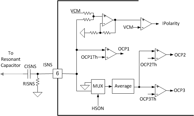
The ISNS pin is connected to the resonant capacitor using a high voltage capacitor. The capacitor CISNS and the resistor RISNS form a differentiator. The resonant capacitor voltage is differentiated to get the resonant current. The differentiated signal is AC and goes both positive and negative. In order to sense the zero crossing, the signal is level shifted using an op amp adder. The IPolarity comparator detects the direction of the resonant current. IPolarity is checked at LSON and HSON falling edges for ZCS protection, with more details described in Section 7.3.9.1 section. The digital state machine implements a blanking time on IPolarity. The IPolarity edges during the first 400 ns of dead time are ignored considering the noise on ISNS pin introduced by the switching node transition.
OCP2 and OCP3 thresholds are based on average input current. To get the average input current, the differentiator output is multiplexed with the high-side switch on signal HSON. When HSON is on, the MUX output is the differentiator output; when HSON is off, the MUX output is 0. The MUX output is then averaged using a low pass filter. The output of the filter is the sensed average input current. Note that the MUX needs to pass through both positive and negative voltages. OCP2 and OCP3 faults have a 2 ms and 50 ms timer respectively. Only when the OCP2/OCP3 comparators output high for continuous 2 ms or 50 ms, will the faults be activated.
OCP1 threshold is set on the peak resonant current. The voltage on the ISNS pin gets compared to OCP1 threshold OCP1Th directly. The peak resonant current is checked once per cycle on the positive half cycle. OCP1 fault is only activated when there are 4 consecutive cycles of OCP1 event detected. During start up, the OCP1 comparator output of the first 15 cycles are ignored.
 Figure 7-7 ISNS Block Diagram