ZHCSJY8E june 2019 – february 2021 UCC256402 , UCC256403 , UCC256404
PRODUCTION DATA
- 1 特性
- 2 应用
- 3 说明
- 4 Revision History
- 5 Pin Configuration and Functions
- 6 Specifications
-
7 Detailed Description
- 7.1 Overview
- 7.2 Functional Block Diagram
- 7.3 Feature Description
- 7.4
Device Functional Modes
- 7.4.1 High Voltage Start-Up
- 7.4.2 X-Capacitor Discharge
- 7.4.3 Burst Mode Control
- 7.4.4
System State Machine
-
Application and Implementation
- 8.1 Application Information
- 8.2
Typical Application
- 8.2.1 Design Requirements
- 8.2.2
Detailed Design Procedure
- 8.2.2.1 LLC Power Stage Requirements
- 8.2.2.2 LLC Gain Range
- 8.2.2.3 Select Ln and Qe
- 8.2.2.4 Determine Equivalent Load Resistance
- 8.2.2.5 Determine Component Parameters for LLC Resonant Circuit
- 8.2.2.6 LLC Primary-Side Currents
- 8.2.2.7 LLC Secondary-Side Currents
- 8.2.2.8 LLC Transformer
- 8.2.2.9 LLC Resonant Inductor
- 8.2.2.10 LLC Resonant Capacitor
- 8.2.2.11 LLC Primary-Side MOSFETs
- 8.2.2.12 LLC Rectifier Diodes
- 8.2.2.13 LLC Output Capacitors
- 8.2.2.14 HV Pin Series Resistors
- 8.2.2.15 BLK Pin Voltage Divider
- 8.2.2.16 ISNS Pin Differentiator
- 8.2.2.17 VCR Pin Capacitor Divider
- 8.2.2.18 BW Pin Voltage Divider
- 8.2.2.19 Soft Start and Burst Mode Programming
- 8.2.3 Application Curves
-
Application and Implementation
- 8 Power Supply Recommendations
- 9 Layout
- 10Device and Documentation Support
8.2.2.19 Soft Start and Burst Mode Programming
The LL/SS and BW pins allow the designer to select a burst mode threshold as well as program hysteresis for entering and exiting burst mode. The resistor divider of connected to the LL/SS pin sets the BMTH threshold while the BW pin sets the ratio between BMTL and BMTH. In addition to programming the burst mode threshold, the LL/SS pin provides the capability to program an initial voltage onto the LL/SS pin in order to limit the maximum switching frequency during startup. For initial selection of LL/SS components, it is recommended to select an initial LL/SS pin voltage between 0 V and 1 V and to select burst mode threshold between 1 V and 2 V. The LL/SS pin parameters can be fine tuned later based on bench measurement.
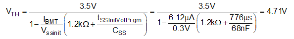
In this design, an initial LL/SS pin voltage of 0.3 V and a BMTH threshold of 0.6 V are selected. The soft start capacitor sets how quickly the voltage on the soft start capacitor rises. The soft start time varies with load condition. At full load or over load condition, the soft start time is the longest. It is not easy to calculate the exact soft start time value. However, it can be estimated that under full load condition, the longest possible soft start time is determined by how quickly the soft start pin voltage rises to the maximum VCR peak to peak voltage. For a start up time of 7.5 ms, the soft start capacitor is sized to be the following:

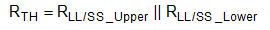
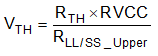
A standard value of 68nF is selected for the soft start capacitor. In order to properly select the resistors on LL/SS, first define RTH as the equivalent resistance on the LL/SS pin and VTH as the equivalent voltage source on the LL/SS pin.
During the SS pull low phase, the voltage on the LL/SS pin is internally pulled down through a 1.2 kΩ resistor. During the SS initial program phase, the internal pulldown is released and the soft start capacitor is allowed to naturally charge up from RVCC. The total voltage offset on the LL/SS soft start capacitor can be calculated using the equation below.
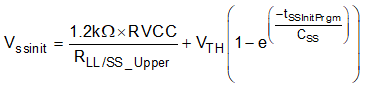
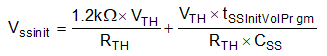
Substituting for RVCC/RLL/SS_Upper and using a linear approximation for the exponential term, the equation can be simplified to the following.
The current used by the LL/SS pin to program BMTH, IBMT, has the following relationships. IBMT can be directly solved for based on the desired BMTH threshold.
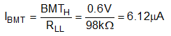
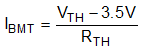
Rearranging Equation 73, VTH and RTH can now be calculated.
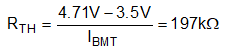
Values for RLL/SS_Upper and RLL/SS_Lower can be determined from VTH and RTH
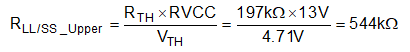
A standard value of 549 kΩ is selected for RLL/SS_Upper.
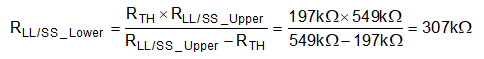
A standard value of 316 kΩ is selected for RLL/SS_Lower.