ZHCSQI2A November 2022 – January 2024 TPS92620-Q1
PRODUCTION DATA
- 1
- 1 特性
- 2 应用
- 3 说明
- 4 Pin Configuration and Functions
- 5 Specifications
-
6 Detailed Description
- 6.1 Overview
- 6.2 Functional Block Diagram
- 6.3
Feature Description
- 6.3.1 Power Supply (SUPPLY)
- 6.3.2 Enable and Shutdow(EN)
- 6.3.3 Constant-Current Output and Setting (INx)
- 6.3.4 Thermal Sharing Resistor (OUTx and RESx)
- 6.3.5 PWM Control (PWMx)
- 6.3.6 Supply Control
- 6.3.7 Diagnostics
- 6.3.8 FAULT Bus Output With One-Fails-All-Fail
- 6.3.9 FAULT Table
- 6.3.10 LED Fault Summary
- 6.3.11 IO Pins Inner Connection
- 6.4 Device Functional Modes
- 7 Application and Implementation
- 8 Device and Documentation Support
- 9 Revision History
- 10Mechanical, Packaging, and Orderable Information
封装选项
机械数据 (封装 | 引脚)
散热焊盘机械数据 (封装 | 引脚)
- DRR|12
订购信息
6.3.3 Constant-Current Output and Setting (INx)
The TPS92620-Q1 device is a high-side current driver for driving LEDs. The device controls each output current through regulating the voltage drop on an external high-side current-sense resistor, R(SNSx) independently for each channel. An integrated error amplifier drives an internal power transistor to maintain the voltage drop on the current-sense resistor R(SNSx) to V(CS_REG) and therefore regulates the current output to target value. When the output current is in regulation, use Equation 1 to calculate the current value for each channel.
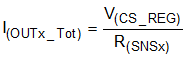
where
- V(CS_REG) = 150mV
- x = 1, or 2 for output channel 1 or 2
When the supply voltage drops below total LED string forward voltage plus required headroom voltage, the sum of V(DROPOUT) and V(CS_REG), the TPS92620-Q1 is not able to deliver enough current output as set by the value of R(SNSx), and the voltage across the current-sense resistor R(SNSx) is less than V(CS_REG).