ZHCSQI2A November 2022 – January 2024 TPS92620-Q1
PRODUCTION DATA
- 1
- 1 特性
- 2 应用
- 3 说明
- 4 Pin Configuration and Functions
- 5 Specifications
-
6 Detailed Description
- 6.1 Overview
- 6.2 Functional Block Diagram
- 6.3
Feature Description
- 6.3.1 Power Supply (SUPPLY)
- 6.3.2 Enable and Shutdow(EN)
- 6.3.3 Constant-Current Output and Setting (INx)
- 6.3.4 Thermal Sharing Resistor (OUTx and RESx)
- 6.3.5 PWM Control (PWMx)
- 6.3.6 Supply Control
- 6.3.7 Diagnostics
- 6.3.8 FAULT Bus Output With One-Fails-All-Fail
- 6.3.9 FAULT Table
- 6.3.10 LED Fault Summary
- 6.3.11 IO Pins Inner Connection
- 6.4 Device Functional Modes
- 7 Application and Implementation
- 8 Device and Documentation Support
- 9 Revision History
- 10Mechanical, Packaging, and Orderable Information
封装选项
机械数据 (封装 | 引脚)
散热焊盘机械数据 (封装 | 引脚)
- DRR|12
订购信息
6.3.6 Supply Control
The TPS92620-Q1 can support supply control to turn ON and OFF output current. When the voltage applied on the SUPPLY pin is higher than the LED string forward voltage plus needed headroom voltage at required current, and the PWM pin voltage is high, the output current is turned ON and well regulated. However, if the voltage applied on the SUPPLY pin is lower than V(POR_falling), the output current is turned OFF. With this feature, the power supply voltage in designed pattern can control the output current ON and OFF. The brightness is adjustable if the ON and OFF frequency is fast enough. Because of the high accuracy design of PWM threshold in TPS92620-Q1, TI recommends a resistor divider on the PWM pin to set the SUPPLY threshold higher than LED forward voltage plus required headroom voltage as shown in Figure 6-2. The headroom voltage is basically the summation of V(DROPOUT) and V(CS_REG). When the voltage on the PWM pin is higher than VIH(PWM), the output current is turned ON. However, when the voltage on the PWM is lower than VIL(PWM), the output current is turned OFF. Use Equation 2 to calculate the SUPPLY threshold voltage.
 Figure 6-2 Application Schematic for Supply Control LED Brightness
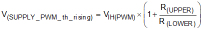
where
- VIH(PWM) = 1.26V (maximum)