ZHCSL68C April 2017 – December 2020 TPS7A84A
PRODUCTION DATA
- 1 特性
- 2 应用
- 3 说明
- 4 Revision History
- 5 Pin Configuration and Functions
-
6 Specifications
- 6.1 Absolute Maximum Ratings
- 6.2 ESD Ratings
- 6.3 Recommended Operating Conditions
- 6.4 Thermal Information
- 6.5 Electrical Characteristics: General
- 6.6 Electrical Characteristics: TPS7A8400A
- 6.7 Electrical Characteristics: TPS7A8401A
- 6.8 Typical Characteristics: TPS7A8400A
- 6.9 Typical Characteristics: TPS7A8401A
- 7 Detailed Description
-
8 Application and Implementation
- 8.1
Application Information
- 8.1.1
External Component Selection
- 8.1.1.1 Adjustable Operation
- 8.1.1.2 ANY-OUT Programmable Output Voltage
- 8.1.1.3 ANY-OUT Operation
- 8.1.1.4 Increasing ANY-OUT Resolution for LILO Conditions
- 8.1.1.5 Current Sharing
- 8.1.1.6 Recommended Capacitor Types
- 8.1.1.7 Input and Output Capacitor Requirements (CIN and COUT)
- 8.1.1.8 Feed-Forward Capacitor (CFF)
- 8.1.1.9 Noise-Reduction and Soft-Start Capacitor (CNR/SS)
- 8.1.2 Start-Up
- 8.1.3 AC and Transient Performance
- 8.1.4 DC Performance
- 8.1.5 Sequencing Requirements
- 8.1.6 Negatively Biased Output
- 8.1.7 Reverse Current Protection
- 8.1.8 Power Dissipation (PD)
- 8.1.1
External Component Selection
- 8.2 Typical Applications
- 8.1
Application Information
- 9 Power Supply Recommendations
- 10Layout
- 11Device and Documentation Support
8.1.1.1 Adjustable Operation
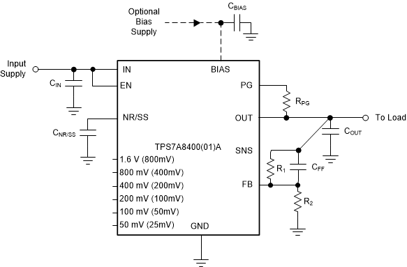
The TPS7A84A can be used either with the internal ANY-OUT network or by using external resistors. Using the ANY-OUT network allows the TPS7A8400A to be programmed from 0.8 V to 3.95 V and from 0.5 V to 2.075 V for the TPS7A8401A. For an output voltage range greater than 2.075 V for the TPS7A8401A and 3.95 V for the TPS7A8400A and up to 5.15 V, external resistors must be used. This configuration is referred to as the adjustable configuration of the TPS7A84A throughout this document. The output voltage is set by two resistors, as shown in Figure 8-1. 0.75% accuracy can be achieved with an external BIAS for VIN lower than 2.2 V.
 Figure 8-1 Adjustable Operation
R1 and R2 can be calculated for any output voltage range using Equation 1. This resistive network must provide a current equal to or greater than 5 μA for dc accuracy. TI recommends using an R1 approximately 12 kΩ to optimize the noise and PSRR.
Table 8-1 shows the resistor combinations required to achieve several common rails using standard 1%-tolerance resistors.
| TARGETED OUTPUT VOLTAGE (V) | FEEDBACK RESISTOR VALUES | CALCULATED OUTPUT VOLTAGE (V) | |
|---|---|---|---|
| R1 (kΩ) | R2 (kΩ) | ||
| 0.9 | 12.4 | 100 | 0.899 |
| 0.95 | 12.4 | 66.5 | 0.949 |
| 1.00 | 12.4 | 49.9 | 0.999 |
| 1.10 | 12.4 | 33.2 | 1.099 |
| 1.20 | 12.4 | 24.9 | 1.198 |
| 1.50 | 12.4 | 14.3 | 1.494 |
| 1.80 | 12.4 | 10 | 1.798 |
| 1.90 | 12.1 | 8.87 | 1.89 |
| 2.50 | 12.4 | 5.9 | 2.48 |
| 2.85 | 12.1 | 4.75 | 2.838 |
| 3.00 | 12.1 | 4.42 | 2.990 |
| 3.30 | 11.8 | 3.74 | 3.324 |
| 3.60 | 12.1 | 3.48 | 3.582 |
| 4.5 | 11.8 | 2.55 | 4.502 |
| 5.00 | 12.4 | 2.37 | 4.985 |
| TARGETED OUTPUT VOLTAGE (V) | FEEDBACK RESISTOR VALUES | CALCULATED OUTPUT VOLTAGE (V) | |
|---|---|---|---|
| R1 (kΩ) | R2 (kΩ) | ||
| 0.6 | 11 | 54.9 | 0.600 |
| 0.7 | 10.2 | 25.5 | 0.700 |
| 0.75 | 10 | 20 | 0.750 |
| 0.8 | 10.7 | 17.8 | 0.800 |
| 0.9 | 11 | 13.7 | 0.901 |
| 1.0 | 9.09 | 9.09 | 1.000 |
| 1.05 | 11 | 10 | 1.050 |
| 1.1 | 10.7 | 8.87 | 1.103 |
| 1.2 | 9.31 | 6.65 | 1.200 |
| 1.5 | 11 | 5.49 | 1.502 |
| 1.8 | 10.2 | 3.92 | 1.801 |
| 3.30 | 10.7 | 1.91 | 3.301 |
| 5.00 | 10.2 | 1.13 | 5.013 |