ZHCSL68C April   2017  – December 2020 TPS7A84A

PRODUCTION DATA  

  1. 特性
  2. 应用
  3. 说明
  4. Revision History
  5. Pin Configuration and Functions
  6. Specifications
    1. 6.1 Absolute Maximum Ratings
    2. 6.2 ESD Ratings
    3. 6.3 Recommended Operating Conditions
    4. 6.4 Thermal Information
    5. 6.5 Electrical Characteristics: General
    6. 6.6 Electrical Characteristics: TPS7A8400A
    7. 6.7 Electrical Characteristics: TPS7A8401A
    8. 6.8 Typical Characteristics: TPS7A8400A
    9. 6.9 Typical Characteristics: TPS7A8401A
  7. Detailed Description
    1. 7.1 Overview
    2. 7.2 Functional Block Diagrams
    3. 7.3 Feature Description
      1. 7.3.1 Voltage Regulation Features
        1. 7.3.1.1 DC Regulation
        2. 7.3.1.2 AC and Transient Response
      2. 7.3.2 System Start-Up Features
        1. 7.3.2.1 Programmable Soft Start (NR/SS)
        2. 7.3.2.2 Internal Sequencing
          1. 7.3.2.2.1 Enable (EN)
          2. 7.3.2.2.2 Undervoltage Lockout (UVLO) Control
          3. 7.3.2.2.3 Active Discharge
        3. 7.3.2.3 Power-Good Output (PG)
      3. 7.3.3 Internal Protection Features
        1. 7.3.3.1 Foldback Current Limit (ICL)
        2. 7.3.3.2 Thermal Protection (Tsd)
    4. 7.4 Device Functional Modes
      1. 7.4.1 Regulation
      2. 7.4.2 Disabled
  8. Application and Implementation
    1. 8.1 Application Information
      1. 8.1.1 External Component Selection
        1. 8.1.1.1 Adjustable Operation
        2. 8.1.1.2 ANY-OUT Programmable Output Voltage
        3. 8.1.1.3 ANY-OUT Operation
        4. 8.1.1.4 Increasing ANY-OUT Resolution for LILO Conditions
        5. 8.1.1.5 Current Sharing
        6. 8.1.1.6 Recommended Capacitor Types
        7. 8.1.1.7 Input and Output Capacitor Requirements (CIN and COUT)
        8. 8.1.1.8 Feed-Forward Capacitor (CFF)
        9. 8.1.1.9 Noise-Reduction and Soft-Start Capacitor (CNR/SS)
      2. 8.1.2 Start-Up
        1. 8.1.2.1 Circuit Soft-Start Control (NR/SS)
          1. 8.1.2.1.1 Inrush Current
        2. 8.1.2.2 Undervoltage Lockout (UVLO)
        3. 8.1.2.3 Power-Good (PG) Function
      3. 8.1.3 AC and Transient Performance
        1. 8.1.3.1 Power-Supply Rejection Ratio (PSRR)
        2. 8.1.3.2 Output Voltage Noise
        3. 8.1.3.3 Optimizing Noise and PSRR
          1. 8.1.3.3.1 Charge Pump Noise
        4. 8.1.3.4 Load Transient Response
      4. 8.1.4 DC Performance
        1. 8.1.4.1 Output Voltage Accuracy (VOUT)
        2. 8.1.4.2 Dropout Voltage (VDO)
          1. 8.1.4.2.1 Behavior When Transitioning From Dropout Into Regulation
      5. 8.1.5 Sequencing Requirements
      6. 8.1.6 Negatively Biased Output
      7. 8.1.7 Reverse Current Protection
      8. 8.1.8 Power Dissipation (PD)
        1. 8.1.8.1 Estimating Junction Temperature
        2. 8.1.8.2 Recommended Area for Continuous Operation (RACO)
    2. 8.2 Typical Applications
      1. 8.2.1 Low-Input, Low-Output (LILO) Voltage Conditions
        1. 8.2.1.1 Design Requirements
        2. 8.2.1.2 Detailed Design Procedure
        3. 8.2.1.3 Application Curves
  9. Power Supply Recommendations
  10. 10Layout
    1. 10.1 Layout Guidelines
    2. 10.2 Layout Example
  11. 11Device and Documentation Support
    1. 11.1 Device Support
      1. 11.1.1 Development Support
        1. 11.1.1.1 Evaluation Models
        2. 11.1.1.2 Spice Models
    2. 11.2 Documentation Support
      1. 11.2.1 Related Documentation
    3. 11.3 接收文档更新通知
    4. 11.4 支持资源
    5. 11.5 Trademarks
    6. 11.6 静电放电警告
    7. 11.7 术语表

封装选项

机械数据 (封装 | 引脚)
散热焊盘机械数据 (封装 | 引脚)
订购信息

Estimating Junction Temperature

The JEDEC standard now recommends the use of psi (Ψ) thermal metrics to estimate the junction temperatures of the LDO when in-circuit on a typical PCB board application. These metrics are not strictly speaking thermal resistances, but rather offer practical and relative means of estimating junction temperatures. These psi metrics are determined to be significantly independent of the copper-spreading area. The key thermal metrics (ΨJT and ΨJB) are given in the Thermal Information table in the Section 6 section and are used in accordance with Equation 14.
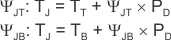
Equation 14. GUID-D714EBFB-F6F2-4588-94BD-3A06C08D76D9-low.gif

where:

  • PD is the power dissipated as explained in Equation 11
  • TT is the temperature at the center-top of the device package, and
  • TB is the PCB surface temperature measured 1 mm from the device package and centered on the package edge