ZHCSL68C April 2017 – December 2020 TPS7A84A
PRODUCTION DATA
- 1 特性
- 2 应用
- 3 说明
- 4 Revision History
- 5 Pin Configuration and Functions
-
6 Specifications
- 6.1 Absolute Maximum Ratings
- 6.2 ESD Ratings
- 6.3 Recommended Operating Conditions
- 6.4 Thermal Information
- 6.5 Electrical Characteristics: General
- 6.6 Electrical Characteristics: TPS7A8400A
- 6.7 Electrical Characteristics: TPS7A8401A
- 6.8 Typical Characteristics: TPS7A8400A
- 6.9 Typical Characteristics: TPS7A8401A
- 7 Detailed Description
-
8 Application and Implementation
- 8.1
Application Information
- 8.1.1
External Component Selection
- 8.1.1.1 Adjustable Operation
- 8.1.1.2 ANY-OUT Programmable Output Voltage
- 8.1.1.3 ANY-OUT Operation
- 8.1.1.4 Increasing ANY-OUT Resolution for LILO Conditions
- 8.1.1.5 Current Sharing
- 8.1.1.6 Recommended Capacitor Types
- 8.1.1.7 Input and Output Capacitor Requirements (CIN and COUT)
- 8.1.1.8 Feed-Forward Capacitor (CFF)
- 8.1.1.9 Noise-Reduction and Soft-Start Capacitor (CNR/SS)
- 8.1.2 Start-Up
- 8.1.3 AC and Transient Performance
- 8.1.4 DC Performance
- 8.1.5 Sequencing Requirements
- 8.1.6 Negatively Biased Output
- 8.1.7 Reverse Current Protection
- 8.1.8 Power Dissipation (PD)
- 8.1.1
External Component Selection
- 8.2 Typical Applications
- 8.1
Application Information
- 9 Power Supply Recommendations
- 10Layout
- 11Device and Documentation Support
7.3.2.3 Power-Good Output (PG)
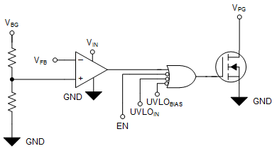
The PG signal provides an easy solution to meet demanding sequencing requirements because PG signals when the output nears its nominal value. PG can be used to signal other devices in a system when the output voltage is near, at, or above the set output voltage (VOUT(nom)). A simplified schematic is shown in Figure 7-6.
The PG signal is an open-drain digital output that requires a pullup resistor to a voltage source and is active high. The PG circuit sets the PG pin into a high-impedance state to indicate that the power is good.
Using a large feed-forward capacitor (CFF) delays the output voltage and, because the PG circuit monitors the FB pin, the PG signal can indicate a false positive. A simple solution to this scenario is to use an external voltage detector device, such as the TPS3890; see the Section 8.1.1.8 section for more information.
 Figure 7-6 Simplified PG Circuit