ZHCSPG4D december 2021 – august 2023 TPS7A14
PRODUCTION DATA
- 1
- 1特性
- 2应用
- 3说明
- 4Revision History
- 5Pin Configuration and Functions
- 6Specifications
- 7Detailed Description
-
8Application and Implementation
- 8.1
Application Information
- 8.1.1 Recommended Capacitor Types
- 8.1.2 Input, Output, and Bias Capacitor Requirements
- 8.1.3 Dropout Voltage
- 8.1.4 Behavior During Transition From Dropout Into Regulation
- 8.1.5 Device Enable Sequencing Requirement
- 8.1.6 Load Transient Response
- 8.1.7 Undervoltage Lockout Circuit Operation
- 8.1.8 Power Dissipation (PD)
- 8.1.9 Estimating Junction Temperature
- 8.1.10 Recommended Area for Continuous Operation
- 8.2 Typical Application
- 8.3 Power Supply Recommendations
- 8.4 Layout
- 8.1
Application Information
- 9Device and Documentation Support
- Mechanical, Packaging, and Orderable Information
封装选项
请参考 PDF 数据表获取器件具体的封装图。
机械数据 (封装 | 引脚)
- DRV|6
- YBK|6
散热焊盘机械数据 (封装 | 引脚)
订购信息
8.1.7 Undervoltage Lockout Circuit Operation
The VIN UVLO circuit makes sure that the regulator remains disabled when the input supply voltage is below the minimum operational voltage range, and makes sure that the regulator shuts down when the input supply collapses. Similarly, the VBIAS UVLO circuit makes sure that the regulator remains disabled when the bias supply voltage is less than the minimum operational voltage range, and makes sure that the regulator shuts down when the bias supply collapses.
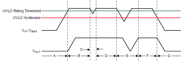
Figure 8-2 shows the UVLO circuit response to various input or bias voltage events. The diagram can be separated into the following parts:
- Region A: The output remains off while the input or bias voltage is below the UVLO rising threshold
- Region B: Normal operation, regulating device
- Region C: Brownout event above the UVLO falling threshold (UVLO rising threshold – UVLO hysteresis). The output can possibly fall out of regulation but the device remains enabled.
- Region D: Normal operation, regulating device
- Region E: Brownout event below the UVLO falling threshold. The device is disabled in most cases and the output falls as a result of the load and active discharge circuit. The device is re-enabled when the UVLO rising threshold is reached and a normal start up follows.
- Region F: Normal operation followed by the input or bias falling to the UVLO falling threshold
- Region G: The device is disabled when the input or bias voltages fall below the UVLO falling threshold to 0 V. The output falls as a result of the load and active discharge circuit.
 Figure 8-2 Typical VIN or VBIAS UVLO Circuit Operation