ZHCSKI6W January 2006 – August 2025 TPS737
PRODUCTION DATA
封装选项
机械数据 (封装 | 引脚)
散热焊盘机械数据 (封装 | 引脚)
订购信息
7.5.1.1 功率耗散
了解器件功率耗散并正确确定连接到接片或焊盘的热平面尺寸,对于避免热关断并提供可靠运行至关重要。
器件的功率耗散取决于输入电压和负载条件,可以使用 方程式 6 计算:
方程式 6. 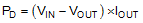
通过使用实现所需输出电压的最低可能输入电压可大大减小功率耗散并提高效率。
在 VSON (DRB) 和 WSON (DRV) 封装上,主要的热传导路径是通过外露焊盘到印刷电路板 (PCB)。焊盘可以接地或保持悬空;但必须将焊盘连接到适当大小的覆铜 PCB 区域,确保器件不会过热。在 SOT-223 (DCQ) 封装上,主要的热传导路径是通过接片到 PCB。接片必须连接到地。最大结至环境热阻取决于最高环境温度、最高器件结温和器件的功率耗散,可以使用 方程式 7 计算:
方程式 7. 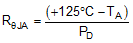
已知最大 RθJA,可以使用 图 7-9 估算适当散热所需的 PCB 覆铜面积最小值。

电路板尺寸为 9in2(即 3in × 3in)时的 RθJA 值是 JEDEC 标准。
图 7-9 RθJA 与电路板尺寸之间的关系图 7-9 展示了 RθJA 与电路板中接地平面覆铜区的函数关系。图 7-9 仅用作参考,演示接地平面中散热的影响,不用于估算实际应用环境中的实际热性能。
注:
器件安装在应用 PCB 上时,强烈建议使用 ΨJT 和 ΨJB,参见热性能信息表中的说明。