ZHCSNX8B December 2020 – September 2023 TPS6593-Q1
PRODUCTION DATA
- 1
- 1 特性
- 2 应用
- 3 说明
- 4 Revision History
- 5 说明(续)
- 6 Pin Configuration and Functions
-
7 Specifications
- 7.1 Absolute Maximum Ratings
- 7.2 ESD Ratings
- 7.3 Recommended Operating Conditions
- 7.4 Thermal Information
- 7.5 General Purpose Low Drop-Out Regulators (LDO1, LDO2, LDO3)
- 7.6 Low Noise Low Drop-Out Regulator (LDO4)
- 7.7 Internal Low Drop-Out Regulators (LDOVRTC, LDOVINT)
- 7.8 BUCK1, BUCK2, BUCK3, BUCK4 and BUCK5 Regulators
- 7.9 Reference Generator (BandGap)
- 7.10 Monitoring Functions
- 7.11 Clocks, Oscillators, and PLL
- 7.12 Thermal Monitoring and Shutdown
- 7.13 System Control Thresholds
- 7.14 Current Consumption
- 7.15 Backup Battery Charger
- 7.16 Digital Input Signal Parameters
- 7.17 Digital Output Signal Parameters
- 7.18 I/O Pullup and Pulldown Resistance
- 7.19 I2C Interface
- 7.20 Serial Peripheral Interface (SPI)
- 7.21 Typical Characteristics
-
8 Detailed Description
- 8.1 Overview
- 8.2 Functional Block Diagram
- 8.3
Feature Description
- 8.3.1 System Supply Voltage Monitor
- 8.3.2
Power Resources (Bucks and LDOs)
- 8.3.2.1
Buck Regulators
- 8.3.2.1.1 BUCK Regulator Overview
- 8.3.2.1.2 Multi-Phase Operation and Phase-Adding or Shedding
- 8.3.2.1.3 Transition Between PWM and PFM Modes
- 8.3.2.1.4 Multi-Phase BUCK Regulator Configurations
- 8.3.2.1.5 Spread-Spectrum Mode
- 8.3.2.1.6 Adaptive Voltage Scaling (AVS) and Dynamic Voltage Scaling (DVS) Support
- 8.3.2.1.7 BUCK Output Voltage Setting
- 8.3.2.1.8 BUCK Regulator Current Limit
- 8.3.2.1.9 SW_Bx Short-to-Ground Detection
- 8.3.2.1.10 Sync Clock Functionality
- 49
- 8.3.2.2 Low Dropout Regulators (LDOs)
- 8.3.2.1
Buck Regulators
- 8.3.3 Output Voltage Monitor and PGOOD Generation
- 8.3.4 Thermal Monitoring
- 8.3.5 Backup Supply Power-Path
- 8.3.6 General-Purpose I/Os (GPIO Pins)
- 8.3.7 nINT, EN_DRV, and nRSTOUT Pins
- 8.3.8 Interrupts
- 8.3.9 RTC
- 8.3.10
Watchdog (WDOG)
- 8.3.10.1 Watchdog Fail Counter and Status
- 8.3.10.2 Watchdog Start-Up and Configuration
- 8.3.10.3 MCU to Watchdog Synchronization
- 8.3.10.4 Watchdog Disable Function
- 8.3.10.5 Watchdog Sequence
- 8.3.10.6 Watchdog Trigger Mode
- 8.3.10.7 WatchDog Flow Chart and Timing Diagrams in Trigger Mode
- 79
- 8.3.10.8 Watchdog Question-Answer Mode
- 8.3.11 Error Signal Monitor (ESM)
- 8.4
Device Functional Modes
- 8.4.1
Device State Machine
- 8.4.1.1 Fixed Device Power FSM
- 8.4.1.2
Pre-Configurable Mission States
- 8.4.1.2.1
PFSM Commands
- 8.4.1.2.1.1 REG_WRITE_IMM Command
- 8.4.1.2.1.2 REG_WRITE_MASK_IMM Command
- 8.4.1.2.1.3 REG_WRITE_MASK_PAGE0_IMM Command
- 8.4.1.2.1.4 REG_WRITE_BIT_PAGE0_IMM Command
- 8.4.1.2.1.5 REG_WRITE_WIN_PAGE0_IMM Command
- 8.4.1.2.1.6 REG_WRITE_VOUT_IMM Command
- 8.4.1.2.1.7 REG_WRITE_VCTRL_IMM Command
- 8.4.1.2.1.8 REG_WRITE_MASK_SREG Command
- 8.4.1.2.1.9 SREG_READ_REG Command
- 8.4.1.2.1.10 SREG_WRITE_IMM Command
- 8.4.1.2.1.11 WAIT Command
- 8.4.1.2.1.12 DELAY_IMM Command
- 8.4.1.2.1.13 DELAY_SREG Command
- 8.4.1.2.1.14 TRIG_SET Command
- 8.4.1.2.1.15 TRIG_MASK Command
- 8.4.1.2.1.16 END Command
- 8.4.1.2.2 Configuration Memory Organization and Sequence Execution
- 8.4.1.2.3 Mission State Configuration
- 8.4.1.2.4 Pre-Configured Hardware Transitions
- 8.4.1.2.1
PFSM Commands
- 8.4.1.3 Error Handling Operations
- 8.4.1.4 Device Start-up Timing
- 8.4.1.5 Power Sequences
- 8.4.1.6 First Supply Detection
- 8.4.1.7 Register Power Domains and Reset Levels
- 8.4.2 Multi-PMIC Synchronization
- 8.4.1
Device State Machine
- 8.5 Control Interfaces
- 8.6 Configurable Registers
- 8.7 Register Maps
- 9 Application and Implementation
- 10Device and Documentation Support
- 11Mechanical, Packaging, and Orderable Information
8.4.2 Multi-PMIC Synchronization
A multi-PMIC synchronization scheme is implemented in the TPS6593-Q1 device to synchronize the power state changes with other PMIC devices. This feature consolidates and simplifies the IO control signals required between the application processor or the microcontroller and multiple PMICs in the system. The control interface consists of an SPMI protocol that communicates the next power state information from the primary PMIC to up to 5 secondary PMICs, and receives feedback signal from the secondary PMICs to indicate any error condition or power state information. Figure 8-43 is the block diagram of the power state synchronization scheme. The primary PMIC in this block diagram is responsible for broadcasting the synchronous system power state data, and processing the error feedback signals from the secondary PMICs. The primary PMIC is the controller device on the SPMI bus, and the secondary PMICs are the target devices on the SPMI bus.
 Figure 8-43 Multi-PMIC Power State
Synchronization Block Diagram
Figure 8-43 Multi-PMIC Power State
Synchronization Block DiagramIn this scheme, each primary and secondary PMIC runs on its own system clock, and maintains its own register map. Each PMIC monitors its own activities and pulls down the open-drain output of nINT or PGOOD pin when errors are detected. The microprocessor must read the status bits from each PMIC device through the I2C or SPI interface to find out the source of the error that is reported.
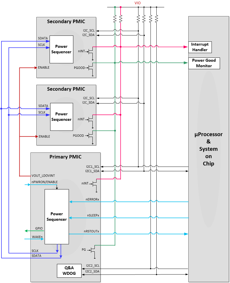
To synchronize the timing when entering and exiting from the LP_STANDBY state, the VOUT_LDOVINT of the TPS6593-Q1 device must be connected to the ENABLE input of the secondary PMICs, which are the target devices in the SPMI interface bus. Figure 8-44 illustrates the pin connections between the primary, the secondary, and the application processor or the System-on-Chip.
 Figure 8-44 Multi-PMIC Pin
Connections
Figure 8-44 Multi-PMIC Pin
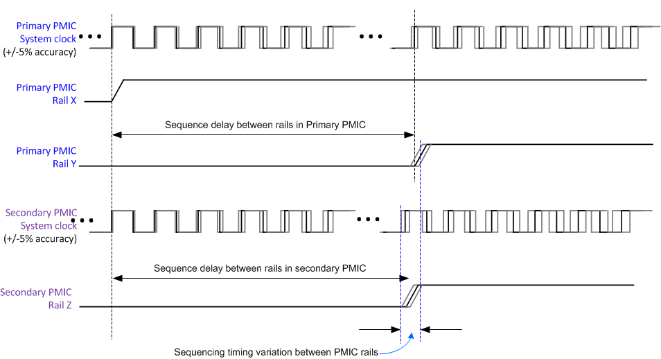
ConnectionsThe power sequencer of the multiple PMICs are synchronized at the beginning of each power up and power down sequence; a variation in the sequence timing, however, is still possible due to the ±5% clock accuracy of the independent system clocks on the primary and secondary PMICs. The worst-case sequence timing variation from different PMIC rails is up to ±10% of the target delay time. Figure 8-45 illustrates the creation of this timing variation between PMICs.
 Figure 8-45 Multi-PMIC Rail Sequencing
Timing Variation