ZHCSEF7G December 2014 – February 2019 TPS659037
PRODUCTION DATA.
- 1 器件概述
- 2 修订历史记录
- 3 Pin Configuration and Functions
-
4 Specifications
- 4.1 Absolute Maximum Ratings
- 4.2 ESD Ratings
- 4.3 Recommended Operating Conditions
- 4.4 Thermal Information
- 4.5 Electrical Characteristics: Latch Up Rating
- 4.6 Electrical Characteristics: LDO Regulator
- 4.7 Electrical Characteristics: Dual-Phase (SMPS12 and SMPS45) and Triple-Phase (SMPS123 and SMPS457) Regulators
- 4.8 Electrical Characteristics: Stand-Alone Regulators (SMPS3, SMPS6, SMPS7, SMPS8, and SMPS9)
- 4.9 Electrical Characteristics: Reference Generator (Bandgap)
- 4.10 Electrical Characteristics: 16-MHz Crystal Oscillator, 32-kHz RC Oscillator, and Output Buffers
- 4.11 Electrical Characteristics: DC-DC Clock Sync
- 4.12 Electrical Characteristics: 12-Bit Sigma-Delta ADC
- 4.13 Electrical Characteristics: Thermal Monitoring and Shutdown
- 4.14 Electrical Characteristics: System Control Threshold
- 4.15 Electrical Characteristics: Current Consumption
- 4.16 Electrical Characteristics: Digital Input Signal Parameters
- 4.17 Electrical Characteristics: Digital Output Signal Parameters
- 4.18 Electrical Characteristics: I/O Pullup and Pulldown
- 4.19 I2C Interface Timing Requirements
- 4.20 SPI Timing Requirements
- 4.21 Typical Characteristics
-
5 Detailed Description
- 5.1 Overview
- 5.2 Functional Block Diagram
- 5.3
Feature Description
- 5.3.1 Power Management
- 5.3.2
Power Resources (Step-Down and Step-Up SMPS Regulators, LDOs)
- 5.3.2.1
Step-Down Regulators
- 5.3.2.1.1 Sync Clock Functionality
- 5.3.2.1.2 Output Voltage and Mode Selection
- 5.3.2.1.3 Current Monitoring and Short Circuit Detection
- 5.3.2.1.4 POWERGOOD
- 5.3.2.1.5 DVS-Capable Regulators
- 5.3.2.1.6 Non DVS-Capable Regulators
- 5.3.2.1.7 Step-Down Converters SMPS12 and SMPS123
- 5.3.2.1.8 Step-Down Converter SMPS45 and SMPS457
- 5.3.2.1.9 Step-Down Converters SMPS3, SMPS6, SMPS7, SMPS8, and SMPS9
- 5.3.2.2 LDOs – Low Dropout Regulators
- 5.3.2.1
Step-Down Regulators
- 5.3.3 Long-Press Key Detection
- 5.3.4 RTC
- 5.3.5 GPADC – 12-Bit Sigma-Delta ADC
- 5.3.6 General-Purpose I/Os (GPIO Pins)
- 5.3.7 Thermal Monitoring
- 5.3.8 Interrupts
- 5.3.9 Control Interfaces
- 5.3.10 Device Identification
- 5.4 Device Functional Modes
-
6 Application and Implementation
- 6.1 Application Information
- 6.2
Typical Application
- 6.2.1 Design Requirements
- 6.2.2 Detailed Design Procedure
- 6.2.3 Application Curves
- 7 Power Supply Recommendations
- 8 Layout
- 9 器件和文档支持
- 10机械、封装和可订购信息
6.2.2.7.1 Meeting the Power Down Sequence
To prevent a sequencing violation, it is important to block reverse current and implement a disable signal to the PMIC. A Schottky diode can block reverse current when the input is removed. Additionally, capacitors can help maintain the input voltage level while the power-down sequence occurs. Depending on the system design, there are a couple ways to implement a disable signal.
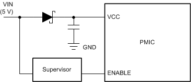
For a system where the TPS659037 is powered by the system input voltage, a supervisor can be used to create a logic signal, indicating if the power is at a good level. An example of this solution is shown in Figure 6-3.
 Figure 6-3 Supporting Uncontrolled Power Down When the PMIC is Supplied by the System Input Voltage
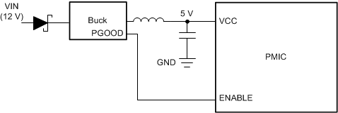
 An alternative solution is possible when a pre-regulator is present. In the case of the pre-regulator, the pre-regulator output capacitance can also act as the energy storage to maintain VCC1 for the necessary time. The total supply capacitance should be calculated to support the worst-case leakage current during power down so that the voltage is maintained until the power-down sequence completes. Figure 6-4 shows an example of this configuration.
 Figure 6-4 Supporting Uncontrolled Power Down when the PMIC is Supplied by a Preregulator
 To determine the capacitance needed at the output of the pre-regulator, use Equation 1. This equation is used to ensure that the power down sequence is complete before the device is disabled.
where
- C is total capacitance on VCC1, including pre-regulator output capacitance and PMIC input capacitance
- I is the total current on the PMIC input supply
- ΔT is the time it takes the power-down sequence to complete
- VCC1 is the voltage at the VCC1 pin
- VSYS_LO is the threshold where the device is disabled