ZHCSJI6 March 2019 TPS65653-Q1
PRODUCT PREVIEW Information. Product in design phase of development. Subject to change or discontinuance without notice.
- 1 特性
- 2 应用
- 3 说明
- 4 修订历史记录
- 5 Pin Configuration and Functions
- 6 Specifications
-
7 Detailed Description
- 7.1 Overview
- 7.2 Functional Block Diagram
- 7.3
Feature Description
- 7.3.1 DC/DC Converters
- 7.3.2 Sync Clock Functionality
- 7.3.3 Power-Up
- 7.3.4 Regulator Control
- 7.3.5 Enable and Disable Sequences
- 7.3.6 Device Reset Scenarios
- 7.3.7 Diagnosis and Protection Features
- 7.3.8 Operation of the GPO Signals
- 7.3.9 Digital Signal Filtering
- 7.4 Device Functional Modes
- 7.5 Programming
- 7.6
Register Maps
- 7.6.1
Register Descriptions
- 7.6.1.1 DEV_REV
- 7.6.1.2 OTP_REV
- 7.6.1.3 BUCK0_CTRL_1
- 7.6.1.4 BUCK0_CTRL_2
- 7.6.1.5 BUCK1_CTRL_1
- 7.6.1.6 BUCK1_CTRL_2
- 7.6.1.7 BUCK0_VOUT
- 7.6.1.8 BUCK1_VOUT
- 7.6.1.9 BUCK0_DELAY
- 7.6.1.10 BUCK1_DELAY
- 7.6.1.11 GPO_DELAY
- 7.6.1.12 GPO2_DELAY
- 7.6.1.13 GPO_CTRL
- 7.6.1.14 CONFIG
- 7.6.1.15 PLL_CTRL
- 7.6.1.16 PGOOD_CTRL_1
- 7.6.1.17 PGOOD_CTRL_2
- 7.6.1.18 PG_FAULT
- 7.6.1.19 RESET
- 7.6.1.20 INT_TOP_1
- 7.6.1.21 INT_TOP_2
- 7.6.1.22 INT_BUCK
- 7.6.1.23 TOP_STAT
- 7.6.1.24 BUCK_STAT
- 7.6.1.25 TOP_MASK_1
- 7.6.1.26 TOP_MASK_2
- 7.6.1.27 BUCK_MASK
- 7.6.1.28 SEL_I_LOAD
- 7.6.1.29 I_LOAD_2
- 7.6.1.30 I_LOAD_1
- 7.6.1
Register Descriptions
- 8 Application and Implementation
- 9 Power Supply Recommendations
- 10Layout
- 11器件和文档支持
7.3.4.1 Enabling and Disabling Regulators
The regulators can be enabled when the device is in STANDBY or ACTIVE state. There are two ways for enable and disable the buck regulators:
- Using BUCKx_EN bit in BUCKx_CTRL_1 register (BUCKx_EN_PIN_CTRL bit is 0 in BUCKx_CTRL_1 register)
- Using EN control pin (BUCKx_EN bit is 1 AND BUCKx_EN_PIN_CTRL bit is 1)
If the EN control pin is used for enable and disable then the delay from the control signal rising edge to start-up is set by BUCKx_STARTUP_DELAY[3:0] bits in BUCKx_DELAY register and the delay from control signal falling edge to shutdown is set by BUCKx_SHUTDOWN_DELAY[3:0] bits in BUCKx_DELAY register. The delays are valid only for EN signal transitions and not for control with I2C writings to the BUCKx_EN bit.
The control of the regulator (with 0-ms delays) is shown in Table 3.
Table 3. Regulator Control
| BUCKx_EN | BUCKx_EN_PIN_CTRL | EN PIN | BUCKx OUTPUT VOLTAGE | |
|---|---|---|---|---|
| Enable/disable control with BUCKx_EN bit | 0 | Don't Care | Don't Care | Disabled |
| 1 | 0 | Don't Care | BUCKx_VSET[7:0] | |
| Enable/disable control with EN pin | 1 | 1 | Low | Disabled |
| 1 | 1 | High | BUCKx_VSET[7:0] |
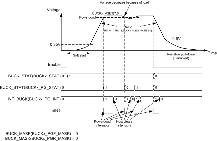
The buck regulator is enabled by the EN pin or by I2C writing as shown in Figure 8. The soft-start circuit limits the in-rush current during start-up. When the output voltage rises to a 0.35-V level, the output voltage becomes slew-rate controlled. If there is a short circuit at the output, and the output voltage does not increase above the 0.35-V level in 1 ms or the output voltage drops below 0.35-V level during operation (for minimum of 1 ms), the regulator is disabled, and BUCKx_SC_INT interrupt in INT_BUCK register is set. When the output voltage reaches the Power-Good threshold level the BUCKx_PG_INT interrupt flag in INT_BUCK register is set. The Power-Good interrupt flag when reaching valid output voltage can be masked using BUCKx_PGR_MASK bit in BUCK_MASK register. The Power-Good interrupt flag can be also generated when the output voltage becomes invalid. The interrupt mask for invalid output voltage detection is set by BUCKx_PGF_MASK bit in BUCK_MASK register. A BUCKx_PG_STAT bit in BUCK_STAT register shows always the validity of the output voltage: 1 means valid and 0 means invalid output voltage. A PGOOD_WINDOW_BUCK bit in PGOOD_CTRL_1 register sets the detection method for the valid buck output voltage, either undervoltage detection or undervoltage and overvoltage detection.
 Figure 8. Buck Regulator Enable and Disable
 The EN input pin has an integrated pulldown resistor. The pulldown resistor is controlled with EN_PD bit in CONFIG register.