ZHCSD49 December 2014 TPS62160-Q1
PRODUCTION DATA.
- 1 特性
- 2 应用
- 3 说明
- 4 简化电路原理图
- 5 修订历史记录
- 6 Pin Configuration and Functions
- 7 Specifications
- 8 Detailed Description
- 9 Application and Implementation
- 10Power Supply Recommendations
- 11Layout
- 12器件和文档支持
- 13机械封装和可订购信息
8 Detailed Description
8.1 Overview
The TPS62160-Q1 synchronous switched mode power converter is based on DCS-Control™ (Direct Control with Seamless transition into power
save mode), an advanced regulation topology, that combines the advantages of hysteretic, voltage mode and current mode control including an AC loop directly associated to the output voltage. This control loop takes information about output voltage changes and feeds it directly to a fast comparator stage. It sets the switching frequency, which is constant for steady state operating conditions, and provides immediate response to dynamic load changes. To get accurate DC load regulation, a voltage feedback loop is used. The internally compensated regulation network achieves fast and stable operation with small external components and low ESR capacitors.
The DCS-Control™ topology supports PWM (Pulse Width Modulation) mode for medium and heavy load conditions and a Power Save Mode at light loads. During PWM, it operates at its nominal switching frequency in continuous conduction mode. This frequency is typically about 2.25 MHz with a controlled frequency variation depending on the input voltage. If the load current decreases, the converter enters Power Save Mode to sustain high efficiency down to very light loads. In Power Save Mode the switching frequency decreases linearly with the load current. Since DCS-Control™ supports both operation modes within one single building block, the transition from PWM to Power Save Mode is seamless without effects on the output voltage.
8.2 Functional Block Diagram
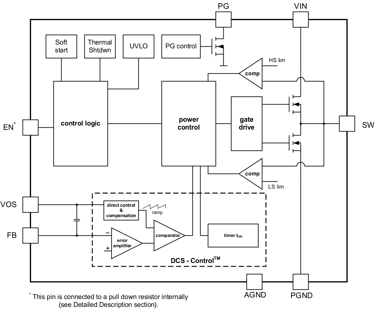
8.3 Feature Description
8.3.1 Enable / Shutdown (EN)
When Enable (EN) is set High, the device starts operation.
Shutdown is forced if EN is pulled Low with a shutdown current of typically 1.5 µA. During shutdown, the internal power MOSFETs as well as the entire control circuitry are turned off. The internal resistive divider pulls down the output voltage smoothly. If the EN pin is Low, an internal pull-down resistor of about 400 kΩ is connected and keeps it Low in case of floating pin.
Connecting the EN pin to an appropriate output signal of another power rail provides sequencing of multiple power rails.
8.3.2 Softstart
The internal soft start circuitry controls the output voltage slope during startup. This avoids excessive inrush current and ensures a controlled output voltage rise time. It also prevents unwanted voltage drops from high-impedance power sources or batteries. When EN is set to start device operation, the device starts switching after a delay of about 50 µs and VOUT rises with a slope of about 25 mV/µs. See Figure 26 and Figure 27 for typical startup operation.
The TPS62160-Q1 can start into a pre-biased output. During monotonic pre-biased startup, the low-side MOSFET is not allowed to turn on until the device's internal ramp sets an output voltage above the pre-bias voltage.
8.3.3 Power Good (PG)
The TPS62160-Q1 has a built in power good (PG) function to indicate whether the output voltage has reached its appropriate level or not. The PG signal can be used for startup sequencing of multiple rails. The PG pin is an open-drain output that requires a pull-up resistor (to any voltage below 7 V). It can sink 2 mA of current and maintain its specified logic low level. It is high impedance when the device is turned off due to EN, UVLO or thermal shutdown.
8.3.4 Under Voltage Lockout (UVLO)
If the input voltage drops, the under voltage lockout prevents misoperation of the device by switching off both the power FETs. The under voltage lockout threshold is set typically to 2.7 V. The device is fully operational for voltages above the UVLO threshold and turns off if the input voltage trips the threshold. The converter starts operation again once the input voltage exceeds the threshold by a hysteresis of typically 180 mV.
8.3.5 Thermal Shutdown
The junction temperature (TJ) of the device is monitored by an internal temperature sensor. If TJ exceeds 160°C (typ), the device goes into thermal shut down. Both the high-side and low-side power FETs are turned off and PG goes high impedance. When TJ decreases below the hysteresis amount, the converter resumes normal operation, beginning with Soft Start. To avoid unstable conditions, a hysteresis of typically 20°C is implemented on the thermal shut down temperature.
8.4 Device Functional Modes
8.4.1 Pulse Width Modulation (PWM) Operation
The TPS62160-Q1 operates with pulse width modulation in continuous conduction mode (CCM) with a nominal switching frequency of about 2.25 MHz. The frequency variation in PWM is controlled and depends on VIN, VOUT and the inductance. The device operates in PWM mode as long the output current is higher than half the inductor's ripple current. To maintain high efficiency at light loads, the device enters Power Save Mode at the boundary to discontinuous conduction mode (DCM). This happens if the output current becomes smaller than half the inductor's ripple current.
8.4.2 Power Save Operation
The TPS62160-Q1's built in Power Save Mode will be entered seamlessly, if the load current decreases. This secures a high efficiency in light load operation. The device remains in Power Save Mode as long as the inductor current is discontinuous.
In Power Save Mode the switching frequency decreases linearly with the load current maintaining high efficiency. The transition into and out of Power Save Mode happens within the entire regulation scheme and is seamless in both directions.
The TPS62160-Q1 includes a fixed on-time circuitry. This on-time, in steady-state operation, can be estimated as:
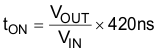
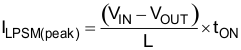
For very small output voltages, the on-time increases beyond the result of Equation 1, to stay above an absolute minimum on-time, tON(min), which is around 80 ns to limit switching losses. The peak inductor current in PSM can be approximated by:
When VIN decreases to typically 15% above VOUT, the TPS62160-Q1 does not enter Power Save Mode, regardless of the load current. The device maintains output regulation in PWM mode.
8.4.3 100% Duty-Cycle Operation
The duty cycle of the buck converter is given by D = Vout/Vin and increases as the input voltage comes close to the output voltage. In this case, the device starts 100% duty cycle operation turning on the high-side switch 100% of the time. The high-side switch stays turned on as long as the output voltage is below the internal set point. This allows the conversion of small input to output voltage differences, e.g. for longest operation time of battery-powered applications. In 100% duty cycle mode, the low-side FET is switched off.
The minimum input voltage to maintain output voltage regulation, depending on the load current and the output voltage level, can be calculated as:
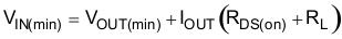
where
IOUT is the output current,
RDS(on) is the RDS(on) of the high-side FET and
RL is the DC resistance of the inductor used.
8.4.4 Current Limit and Short Circuit Protection
The TPS62160-Q1 is protected against heavy load and short circuit events. At heavy loads, the current limit determines the maximum output current. If the current limit is reached, the high-side FET will be turned off. Avoiding shoot through current, the low-side FET will be switched on to sink the inductor current. The high-side FET will turn on again, only if the current in the low-side FET has decreased below the low side current limit threshold.
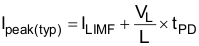
The output current of the device is limited by the current limit (see Electrical Characteristics). Due to internal propagation delay, the actual current can exceed the static current limit during that time. The dynamic current limit can be calculated as follows:
where
ILIMF is the static current limit, specified in the electrical characteristic table,
L is the inductor value,
VL is the voltage across the inductor and
tPD is the internal propagation delay.
The dynamic high side switch peak current can be calculated as follows:

Care on the current limit has to be taken if the input voltage is high and very small inductances are used.
8.4.5 Operation Above TJ = 125°C
The operating junction temperature of the device is specified up to 125°C. In power supply circuits, the self heating effect causes, that the junction temperature, TJ, is even higher than the ambient temperature TA. Depending on TA and the load current, the maximum operating temperature TJ can be exceeded. However, the electrical characteristics are specified up to a TJ of 125°C only. The device operates as long as thermal shutdown threshold is not triggered.